For researchers and engineers, understanding the core specifications of a Scanning Electron Microscope (SEM) is essential for obtaining accurate results. Among the most important parameters are SEM resolution, SEM magnification, and SEM imaging modes. These three factors define the level of detail, scale, and type of information that can be captured from a specimen. Knowing how they work and how they interact helps you select the right SEM for your application.
What is SEM Resolution and Why It Matters
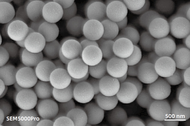
SEM resolution describes the smallest distance between two points that can still be distinguished as separate. It is typically measured in nanometers. Higher SEM resolution means you can capture finer details, which is critical in nanotechnology research, semiconductor inspection, and advanced materials analysis.
The main factors affecting SEM resolution include electron beam spot size, accelerating voltage, electron source type, and vacuum conditions. For example, a field emission SEM generally achieves higher resolution than a thermionic SEM. Low accelerating voltage improves surface detail for delicate samples, while low vacuum operation enables better imaging of non-conductive materials.

Understanding SEM Magnification
SEM magnification is the ratio between the displayed image size and the actual area scanned on the sample. Unlike optical magnification, SEM magnification is controlled electronically by adjusting the scan area. Most modern SEMs offer magnification from about 10x to several hundred thousand times, making it possible to study both large structures and nanoscale features in the same instrument.
The Link Between SEM Resolution and SEM Magnification
While increasing SEM magnification enlarges an image, the level of meaningful detail still depends on the SEM resolution. If the resolution limit is reached, higher magnification will not reveal additional structural details. For example, a system with 1 nm resolution provides much clearer images at high magnification than one limited to 5 nm.
Common SEM Imaging Modes and Their Uses
Modern SEMs feature multiple imaging modes, each designed to provide specific information:
-
Secondary Electron Imaging (SEI) – Delivers high-resolution surface topography, ideal for morphology studies.
-
Backscattered Electron Imaging (BSE) – Reveals compositional contrast based on atomic number differences.
-
Energy Dispersive X-ray Spectroscopy (EDS) – Identifies and quantifies elemental composition.
-
Low Vacuum or Variable Pressure Mode – Allows imaging of non-conductive or hydrated specimens without metal coating.
Switching between different imaging modes enables comprehensive analysis of a single sample.
Choosing an SEM Based on Resolution, Magnification, and Imaging Modes
When selecting an SEM, consider the balance between SEM resolution, SEM magnification range, and available imaging modes. High-resolution capability is essential for nanometer-scale research. A wide magnification range ensures flexibility for different sample sizes, and multiple imaging modes increase versatility for both research and industrial applications.

How CIQTEK SEMs Excel in Resolution, Magnification, and Imaging Modes
CIQTEK SEMs achieve nanometer-scale resolution, allowing users to observe ultra-fine surface features with exceptional clarity. This level of detail is crucial for fields such as semiconductor inspection, nanomaterials research, and precision manufacturing, where accuracy at the smallest scale determines the quality of results.
Flexible Magnification Range
CIQTEK SEMs offer a broad magnification range, enabling smooth transitions from low-magnification overviews to ultra-high-magnification nanoscale imaging. This flexibility allows researchers to locate areas of interest quickly and then zoom in for detailed examination, all without loss of image quality.
Multiple Imaging Modes in One System
CIQTEK SEM systems integrate multiple imaging modes, including secondary electron imaging for surface morphology, backscattered electron imaging for compositional contrast, and low vacuum operation for non-conductive or moisture-sensitive samples. Optional analytical tools, such as EDS, provide elemental composition data. This multi-mode capability means users can conduct comprehensive analyses without switching instruments.
High Value and Cost Efficiency
In addition to technical excellence, CIQTEK SEMs deliver outstanding value. By combining advanced electron optics, reliable hardware, and intuitive software at a competitive price point, we offer one of the best performance-to-cost ratios in the market. Laboratories can access cutting-edge SEM technology while optimizing budget and operational efficiency.