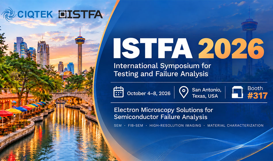
CIQTEK will participate in ISTFA 2026, the 52nd International Symposium for Testing and Failure Analysis, taking place from October 4 to 8 in San Antonio, Texas.
Visit us at Booth #317 to explore CIQTEK SEM and FIB-SEM solutions for semiconductor failure analysis, defect characterization, and advanced electron microscopy. Our U.S. Electron Microscopy Team, including experienced EM Solution Managers, will be on site to discuss your applications and help identify the right microscopy solutions for your lab.
Meet the Failure Analysis Community at ISTFA 2026
Organized by ASM International, ISTFA is a leading international event for microelectronics testing and failure analysis, bringing together engineers, researchers, laboratory professionals, and technology providers from the semiconductor industry.
The conference focuses on real-world challenges in failure analysis, device characterization, microscopy, defect localization, reliability, and related technologies.
SEM for Semiconductor Failure Analysis
As semiconductor devices become smaller and more complex, failure analysis requires high-resolution imaging and reliable information from increasingly fine structures.
CIQTEK offers a range of field emission scanning electron microscopes, including the SEM5000X, SEM5000, and SEM4000Pro, for semiconductor and advanced materials characterization.
Our SEM solutions can support applications such as:
- Semiconductor device and wafer inspection
- Surface defect and morphology analysis
- High-resolution low-kV imaging
- BSE imaging for material contrast
- Particle and contamination analysis
- Electronic components and packaging characterization
Low-kV SEM imaging is especially valuable when examining fine surface structures and sensitive features. Combined with flexible detector options and BSE imaging, it helps researchers obtain both structural and material information from complex samples.
Go Deeper with FIB-SEM
Not every failure can be understood from the surface.
For buried defects, interfaces, and internal structures, FIB-SEM combines focused ion beam processing with high-resolution SEM imaging, enabling targeted cross-section preparation and analysis within the same system.
CIQTEK DB550 FIB-SEM systems support applications including site-specific cross-sectioning, internal defect investigation, multilayer structure analysis, interface characterization, and advanced sample preparation.
This gives failure analysis teams a powerful way to move from locating a problem to investigating what is happening beneath the surface.
Talk with Our U.S. EM Team at Booth #317
Choosing the right electron microscope is not only about specifications. Sample type, imaging requirements, throughput, workflow, chamber capacity, detectors, and future applications all matter.
That is why our U.S. Electron Microscopy Team will be on site at ISTFA 2026, with experienced EM Solution Managers available to answer technical questions and discuss your specific applications.
Whether you are working on semiconductor failure analysis, wafer inspection, low-kV imaging, material contrast, cross-section analysis, or FIB-SEM workflows, we would be happy to talk.
Date: October 4–8, 2026
Location: San Antonio, Texas, USA
CIQTEK Booth: #317
Stop by Booth #317 and meet the CIQTEK U.S. EM Team. See you at ISTFA 2026!