The interface between semiconductor materials and metal electrodes plays a critical role in the performance of electronic devices. Surface morphology, chemical composition, and electronic structure at the interface directly impact key factors such as conductivity, stability, and overall device reliability. Therefore, comprehensive characterization of the semiconductor-metal interface is essential for optimizing device design and improving performance.
Field Emission Scanning Electron Microscopy (FE-SEM) has become a preferred analytical technique due to its high spatial resolution, direct imaging capabilities, and multi-modal analysis features, making it especially suitable for semiconductor-metal interface studies.
SEM Analytical Capabilities
The CIQTEK SEM5000X Field Emission Scanning Electron Microscope demonstrates outstanding performance in the analysis of semiconductor-metal electrode interfaces. Equipped with a Schottky field emission electron gun and an optimized electron optics system, the SEM5000X enables nanoscale high-resolution imaging, capturing fine details of interface morphology, elemental distribution, and electronic properties.
Key Imaging and Analysis Modes:
- Secondary Electron (SE) Imaging: Provides high-resolution surface morphology, ideal for observing roughness, defects, and grain boundaries at the electrode interface.
- Backscattered Electron (BSE) Imaging: Highlights compositional contrast, revealing elemental inhomogeneity and diffusion behavior at the interface.
- Energy Dispersive X-ray Spectroscopy (EDS): Offers qualitative and quantitative elemental analysis, supporting accurate characterization of chemical composition across the interface.
The SEM5000X also supports in-situ heating with MEMS-based heating chips, enabling dynamic studies of material behavior under thermal stress. This is especially useful for observing interdiffusion and reaction zones in real-time during thermal cycling.
Additionally, the system features Electron Beam Induced Current (EBIC) capabilities, allowing for direct evaluation of local electrical properties at the interface, such as carrier lifetime, mobility, and junction activity. This provides valuable data for assessing the electrical performance and reliability of semiconductor devices.
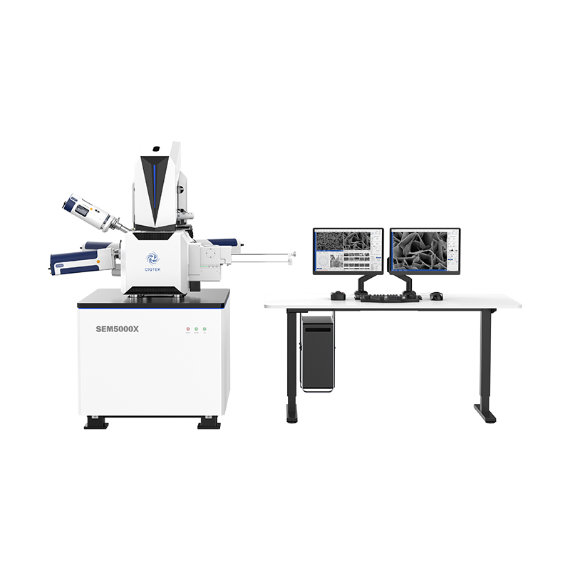
Recommended Product: CIQTEK SEM5000X
For advanced analysis of semiconductor-metal interfaces, CIQTEK strongly recommends the SEM5000X Field Emission SEM. Designed for demanding applications, the SEM5000X offers:
- Ultra-high-resolution imaging down to the nanometer scale
- Comprehensive analytical capabilities including SE/BSE/EDS/EBIC
- Stable performance with user-friendly operation, ideal for both R&D and routine analysis
These features allow researchers to accurately and efficiently characterize the microstructure, composition, and electrical behavior of complex interfaces, ultimately accelerating semiconductor material innovation and device optimization.
The CIQTEK SEM5000X Field Emission Scanning Electron Microscope is a powerful tool for in-depth characterization of semiconductor-metal electrode interfaces. Its high-resolution imaging, multi-modal analysis options, and strong performance stability make it indispensable for materials research, failure analysis, and semiconductor device development.
By enabling clear visualization and precise analysis of interface properties, the SEM5000X contributes to better device design, enhanced performance, and long-term reliability, empowering researchers and engineers in the semiconductor industry.