Recently, a team led by Wang Haomin from the Shanghai Institute of Microsystem and Information Technology of the Chinese Academy of Sciences made significant progress in studying the magnetism of zigzag graphene nanoribbons (zGNRs) using a CIQTEK Scanning Nitrogen-vacancy Microscope (SNVM).
Building on previous research, the team pre-etched hexagonal boron nitride (hBN) with metal particles to create oriented atomic trenches and used a vapor-phase catalytic chemical vapor deposition (CVD) method to controllably prepare chiral graphene nanoribbons in the trenches, obtaining ~9 nm wide zGNRs samples embedded in the hBN lattice. By combining SNVM and magnetic transport measurements, the team directly confirmed its intrinsic magnetism in experiments. This groundbreaking discovery lays a solid foundation for the development of graphene-based spin electronic devices. The related research findings, titled "Signatures of magnetism in zigzag graphene nanoribbons embedded in a hexagonal boron nitride lattice," have been published in the prestigious academic journal "Nature Materials".
Graphene, as a unique two-dimensional material, exhibits magnetic properties of p-orbital electrons that are fundamentally different from the localized magnetic properties of d/f orbital electrons in traditional magnetic materials, opening up new research directions for exploring pure carbon-based magnetism. Zigzag graphene nanoribbons (zGNRs), potentially possessing unique magnetic electronic states near the Fermi level, are believed to hold great potential in the field of spin electronics devices. However, detecting the magnetism of zGNRs through electrical transport methods faces multiple challenges. For instance, nanoribbons assembled from the bottom up are often too short in length to reliably fabricate devices. Additionally, the high chemical reactivity of zGNR edges can lead to instability or uneven doping. Furthermore, in narrower zGNRs, the strong antiferromagnetic coupling of edge states can make it difficult to detect their magnetic signals electrically. These factors hinder direct detection of the magnetism in zGNRs.
ZGNRs embedded in the hBN lattice exhibit higher edge stability and feature an inherent electric field, creating ideal conditions for detecting the magnetism of zGNRs. In the study, the team used CIQTEK's Room-Temperature SNVM to observe the magnetic signals of zGNRs directly at room temperature.
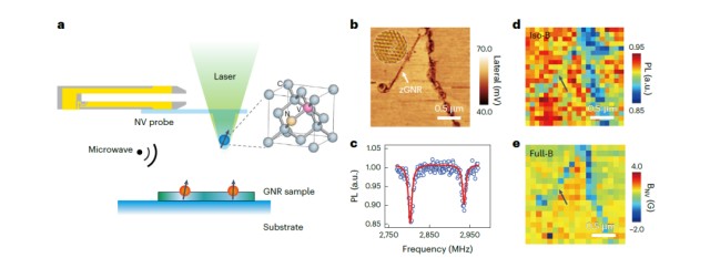
Figure 1: Magnetic measurement of zGNR embedded in a hexagonal boron nitride lattice using Scanning Nitrogen-vacancy Microscope
In electrical transport measurements, the fabricated approximately 9-nanometer-wide zGNR transistors demonstrated high conductivity and ballistic transport characteristics. Under the influence of a magnetic field, the device exhibited significant anisotropic magnetoresistance, with a magnetoresistance change of approximately 175 Ω at 4 K, a magnetoresistance ratio of about 1.3%, and this signal persisted even at temperatures as high as 350 K. Hysteresis was only observed under a magnetic field perpendicular to the plane of the zGNRs, confirming its magnetic anisotropy. Through analysis of the variation of magnetoresistance with tilting angle, the researchers found that the magnetic moment is perpendicular to the sample surface. Furthermore, the decrease in magnetoresistance with increasing source-drain bias and temperature revealed the interaction between magnetic response and charge transport and thermal vibrations.
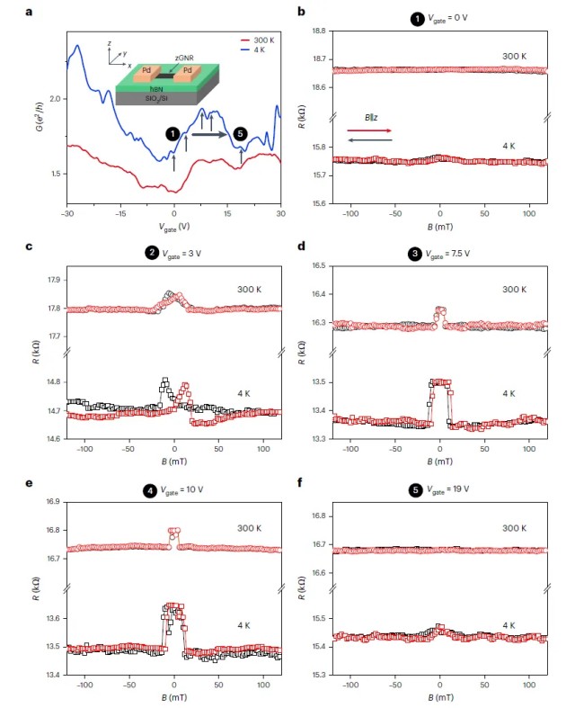
Figure 2: Magnetic transport characteristics of 9-nanometer-wide zGNR devices embedded in hBN
This research, by combining Scanning Nitrogen-vacancy Microscope technology and transport measurements, directly confirmed the existence of intrinsic magnetism in hBN-embedded zGNRs for the first time, providing a possibility for controlling magnetism through an electric field. This work not only deepens the understanding of graphene's magnetic properties but also opens up new pathways for the development of spin electronic devices based on graphene.
Experience the Nano-scale Magnetic Imaging System
CIQTEK invites you to experience the Scanning Nitrogen-vacancy Microscope (SNVM) – a globally leading nano-scale magnetic field imaging system, operating at temperatures of 1.8~300 K with a vector magnetic field of 9/1/1 T, achieving a magnetic spatial resolution of 10 nm, and magnetic sensitivity of 2 μT/Hz1/2.
SNVM is a precision measurement instrument that combines Diamond Nitrogen-vacancy (NV) Optically Detected Magnetic Resonance (ODMR) technology with Atomic Force Microscopy (AFM) scanning imaging technology. It features high spatial resolution, high-sensitivity magnetic imaging, versatile detection capabilities, and non-invasive detection advantages, making it important in areas such as magnetic domain characterization, antiferromagnetic imaging, superconductor characterization, and research on two-dimensional magnetic materials.
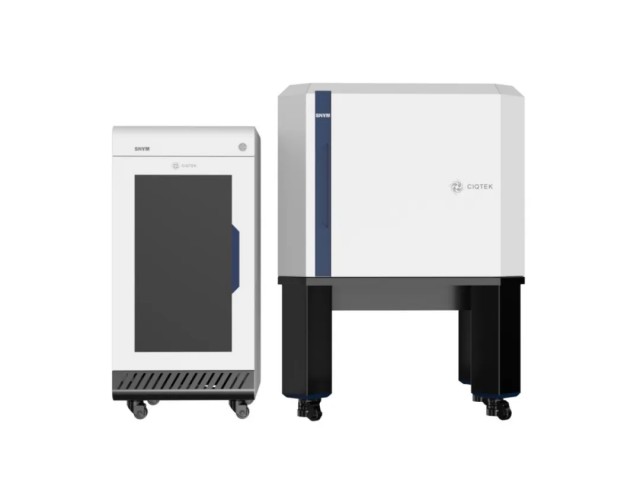
Room temperature version of SNVM
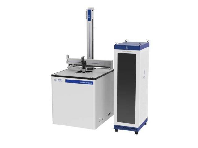
Cryogenic version of SNVM