The biggest difference between capacitive and resistive touch screens is how you use them. You use a capacitive touch screen with your finger. Your skin helps the screen work because it conducts electricity. This type is fast and gives accurate responses. It works well for phones, tablets, and most devices people use every day. A resistive touchscreen works when you press on it. You can use gloves or a stylus with it. This makes resistive screens good for factories and outdoor machines. They are strong and cost less.
When picking a touch screen, think about what you need:
-
Do you want high sensitivity and clear images?
-
Will you use gloves or a stylus?
-
Do you need something that costs less?
-
Will your device be used in tough places?
|
Touch Screen Type
|
Preferred Scenario
|
Key Advantages
|
|
Capacitive
|
Mobile devices, medical computers
|
Accurate, clear, easy to clean
|
|
Resistive
|
Industrial machines, POS systems
|
Strong, works with gloves
|
How Capacitive Touch Screens Work
Capacitive Touch Screen Basics
You use a capacitive touchscreen by touching it with your finger. Your body can carry electricity, and the screen uses this. When you touch the screen, your finger makes a small capacitor with it. The system feels this change and finds where you touched. The screen has a special layer that holds electric charges. Your finger pulls a tiny charge to the spot you touch. The controller checks this change and tells the device where you pressed.
Projected capacitance is used in many new high sensitivity capacitive touch screens. This lets the screen sense more than one touch at once. You can pinch, zoom, or swipe with two or more fingers. You cannot use normal gloves or things that do not carry electricity. You need to use your finger, a special stylus, or gloves made for capacitive screens.
Tip: If you want a screen that reacts fast and works well with your fingers, pick a capacitive touchscreen.
Capacitive Touchscreen Features
Capacitive touch screens are made with strong glass. Many use Gorilla Glass, which is hard to scratch. Some screens have extra layers to stop damage from keys or coins. You see this kind of screen in phones, tablets, and laptops.
Projected capacitance also helps the screen last a long time. Most capacitive touch screens work well for 3 to 10 years. This depends on how much you use them. You get a screen that stays clear and sensitive for years. The glass cover is easy to clean and keeps the screen looking new.
A capacitive touchscreen gives you a smooth and steady experience. You get quick response, clear pictures, and a tough surface for daily use.
How Resistive Touch Screens Work
Resistive Touch Screens Structure
A high accuracy resistive touch screen has layers that help it sense touch. There are two main layers in the screen. The top layer is soft and made of polyester film. The bottom layer is hard and made of glass. Both layers have a thin, clear Indium Tin Oxide coating. Tiny dots keep the layers apart. These dots stop the layers from touching when you do not press.
When you press the screen, the top layer bends down. It touches the bottom layer and makes a small electrical link. This link changes the resistance at that spot. The system checks this change and finds where you pressed. You can use almost anything to press the screen because it works by pressure.
Here is how a resistive touch screen works:
-
You press the soft top layer.
-
The top layer bends and touches the bottom layer.
-
An electrical link forms where you touch.
-
The system checks the change in resistance.
-
The touchscreen finds your touch spot.
Resistive Touch Screens Features
A resistive touch screen has many helpful features. You can use your finger, a stylus, or a gloved hand. This is great for places where gloves or tools are needed. Many people use resistive touch screens in factories, outdoor machines, and medical devices.
Note: A resistive touchscreen works with gloves, styluses, and pens. You do not need special tools.
Resistive touch screens work well in tough places. They handle dirt, moisture, and heavy use. You see them in industrial machines, medical devices, and outdoor controls. Many companies choose large format resistive touch screens because they last long and cost less.
Here is a quick look at how resistive and capacitive screens compare:
|
Screen Type
|
Touch Sensitivity
|
|
Capacitive
|
More sensitive
|
|
Resistive
|
Less sensitive
|
A resistive touch screen is made to be strong and flexible. It works in many places and with many tools. If you need a screen for hard jobs, a resistive touchscreen is a good pick.
A resistive touchscreen gives you steady performance where you need it.
Capacitive vs Resistive Comparison
Sensitivity & Accuracy
A capacitive touchscreen reacts very fast. It can sense even a light touch from your finger. This makes it great for things that need quick and exact moves. You can tap, swipe, or drag, and the screen follows you right away. The screen feels smooth and new.
A resistive touchscreen works in another way. You have to press down with your finger, a stylus, or anything else. The screen does not react as fast as a capacitive one. Sometimes you must press harder or try again. This can slow you down if you want a quick answer.
If you want a screen that feels easy and reacts fast, pick a capacitive touchscreen.
Multi-Touch & Input Methods
How you use each touchscreen changes how it feels. A capacitive touchscreen lets you use more than one finger at once. You can pinch to zoom, turn pictures, or swipe with many fingers. These moves make the screen feel smart and simple.
A resistive touchscreen cannot do as much. It only senses one touch at a time, or maybe two simple points. You cannot do moves like pinch-to-zoom. Some actions are harder or you cannot do them at all.
Here is a table to show the differences:
|
Feature
|
Capacitive Touchscreen
|
Resistive Touchscreen
|
|
Multi-Touch Capability
|
Supports gestures like pinch-to-zoom and rotation
|
Only basic 2-point detection
|
|
Input Methods
|
Fingers, special gloves, special styluses
|
Any object, gloves, or styluses
|
|
User Experience
|
Modern, responsive, smooth
|
Basic, sometimes slow, limited gestures
|
Durability & Longevity
You want your touchscreen to last a long time. A capacitive touchscreen uses strong glass. It does not have moving parts. This makes it tough and hard to scratch. The screen stays sensitive for years. You do not need to fix or reset it often. Most capacitive touchscreens last longer and break less.
A resistive touchscreen has a plastic top layer. This layer can get worn out after a while. Scratches and dents can show up if you use sharp things. You may need to reset the screen after using it a lot. It does not last as long as a capacitive touchscreen, but it still works well in rough places.
Pick a capacitive touchscreen if you want a screen that lasts long and needs little care.
Cost Factors
Price is important when you choose a touchscreen. A capacitive touchscreen costs more than a resistive one. The new technology and extra features make it cost more. You might pay 40-60% more for a capacitive touchscreen with real multitouch.
A resistive touchscreen costs less money. It is a good choice if you need many screens or want to save cash. You get basic touch features for a lower price.
Glove & Stylus Compatibility
Sometimes you need to use your touchscreen with gloves or a stylus. A capacitive touchscreen needs your finger or a special stylus. Normal gloves do not work unless they have a special layer. Some gloves made for touchscreens can wear out or cost more.
A resistive touchscreen works with anything that presses on it. You can use any gloves, styluses, or even a pen cap. This is good for outdoor work, medical jobs, or places where you must wear gloves.
Here is a table to help you compare:
|
Feature
|
Capacitive Touchscreen
|
Resistive Touchscreen
|
|
Glove Compatibility
|
Needs special gloves or bare fingers
|
Works with any gloves
|
|
Stylus Compatibility
|
Needs special stylus
|
Works with any stylus or object
|
|
Industrial Use
|
Limited by glove needs
|
Very flexible, works in all settings
|
If you work in cold, dirty, or tough places, a resistive touchscreen gives you more ways to use it.
Capacitive vs Resistive Comparison: Quick Summary
-
Capacitive touchscreen: Fast, accurate, supports many finger moves, costs more, needs special gloves or stylus, lasts longer.
-
Resistive touchscreen: Works with any object, costs less, handles gloves and styluses, less sensitive, wears out faster.
You can use this comparison to pick the touchscreen that fits you best. Think about how you will use the screen, what you will touch it with, and how much you want to spend.
Pros and Cons of Capacitive Touch Screens
Capacitive Touchscreen Advantages
A capacitive touchscreen gives you many good things. The screen reacts fast when you touch it. You do not have to press hard, so your hands do not get tired. The glass stays clear and bright, so pictures look sharp and colors pop. You can clean the screen easily. It only works with your skin or a special stylus, so you will not tap by mistake.
Here are some advantages of capacitive touchscreens:
-
The glass is strong and does not scratch or break easily.
-
The screen shows bright and sharp images.
-
You can use gestures like pinch-to-zoom or swipe.
-
The screen reacts fast with almost no wait.
-
It is easy to clean and does not get dirty fast.
-
The screen lasts a long time because there are no moving parts.
-
It looks modern and nice on any device.
Tip: If you want a smooth, long-lasting screen that lets you use cool gestures, a capacitive touchscreen is a smart pick.
Capacitive Touchscreen Disadvantages
There are also some downsides to capacitive touchscreens. They do not work with normal gloves or most styluses. You might need to buy special gloves or a special stylus. These screens cost more than other types, so you pay more at first. If the screen gets wet or dirty, it might not work well. The glass can crack if you drop it, but it often still works with small cracks.
Here are some disadvantages of capacitive touchscreens:
-
Does not work with regular gloves or basic styluses.
-
Costs more than resistive screens.
-
May not work well if wet or dirty.
-
Glass can break if dropped, but sometimes still works.
Note: If you need a screen for tough jobs or want to use gloves, you may want to try something else.
Pros and Cons of Resistive Touch Screens
Resistive Touch Screens Advantages
Resistive touchscreens have many good points, especially for tough jobs. These screens work well in places where other screens might not. You can use gloves, a stylus, or any object to touch them. This makes them great for factories, hospitals, and outdoor areas.
Here is a table that shows why people pick resistive touchscreens for hard work:
|
Benefit
|
Description
|
|
Cost-Effectiveness
|
You pay less, especially for big screens.
|
|
Environmental Resilience
|
The screen works in rough places, even with water, dust, or strong signals.
|
|
Proven Reliability
|
This technology has worked well for a long time.
|
|
Precision Input Capability
|
You can use a stylus for very exact tasks.
|
You can use a resistive touchscreen in wet or dirty spots. Workers can keep gloves on and still use the screen. Drivers can enter data without taking off gloves in cold weather. In schools, teachers can make fun lessons, and students with disabilities can use a stylus to help them.
Tip: If you want a screen that works anywhere and with any tool, a resistive touchscreen is a smart pick.
Resistive Touch Screens Disadvantages
There are some things you should know before choosing a resistive touchscreen. These screens need you to press harder to work. You may feel that they are less sensitive than capacitive touchscreens. The display often looks less bright and clear because less light gets through.
Here are some common problems with resistive touchscreens:
-
You need to press harder for your touch to work.
-
The screen usually shows less detail than a capacitive touchscreen.
-
Oil and dirt can build up and make the screen less responsive.
-
The screen lets about 80% of light through, so images look dimmer than the over 90% of a capacitive touchscreen.
Resistive touchscreens can get dirty faster. Oil and dirt can make them work less well. If you want a screen for bright, colorful pictures or quick, light touches, you might like a capacitive touchscreen more.
Note: Think about how you will use your screen. If you want high sensitivity and bright images, a capacitive touchscreen may be better for you.
Best Use Cases for Each Type
Consumer & Mobile Devices
You use a touchscreen when you use your phone or tablet. Most phones and tablets have capacitive touchscreens. These screens feel smooth and react fast to your touch. You can swipe, tap, and zoom with your fingers. This is great for games, social media, and surfing the web. More people buy smartphones every year, so capacitive touchscreens are in most new devices. You see bright colors and sharp pictures, which make videos and photos look awesome.
You get a quick and simple experience with these devices.
Industrial & Outdoor Applications
You need a different touchscreen for tough jobs. Resistive touchscreens work well in factories and outdoor kiosks. You can use gloves or any tool to press the screen. You do not need to worry about rain, dust, or dirt. The screen keeps working even if it gets wet or dirty. This makes resistive touchscreens good for machines in factories, buses, and field equipment.
|
Environment
|
Resistive Touchscreen Performance
|
|
Rain or High Humidity
|
Works well with proper sealing
|
|
Dust and Debris
|
Reliable with proper sealing
|
|
Gloved Operation
|
Any glove material
|
|
Outdoor Use
|
Handles weather and rough handling
|
You can trust these screens to work in hard places.
Medical & Specialized Uses
You see touchscreens in hospitals and labs. Medical devices need screens that work with gloves and can be cleaned with strong chemicals. Resistive touchscreens are good for this because they work with any stylus or glove. Hospitals check for safety and reliability. Devices must follow rules like IEC 60601-1 for safety and ISO 9241-400 for comfort. Some medical screens use capacitive touchscreens for bright images, but many use resistive for easy cleaning and glove use.
You can count on these screens for safe and steady use in medical places.
Decision Checklist for Touch Screens
Choosing the Right Type
You want to pick the best touchscreen for your needs. Start by asking yourself a few simple questions. These questions help you focus on what matters most for your device.
-
Where will you use the touchscreen? If you plan to use it indoors, you can choose almost any type. If you need it for outdoor or factory work, look for a screen that handles dirt, moisture, and big temperature changes.
-
How will you touch the screen? If you use your bare hands, you have more options. If you need to use gloves or a stylus, make sure the touchscreen works with them.
-
Do you need multi-touch? If you want to pinch, zoom, or use more than one finger, pick a screen that supports these moves. If you only need single touches, you can choose a simpler screen.
-
What is your budget? Some touchscreens cost more at first but last longer. Others cost less but may need more care or replacement.
Tip: Think about your work setting, how you will use the screen, and what features matter most to you.
-
Capacitive technology gives you a smooth and easy experience. It works well for phones, tablets, and other devices you use every day.
-
Resistive technology is better for tough jobs. It works with gloves and styluses and handles rough conditions.
Quick Reference Table
Use this table to compare the main features of each touchscreen type. This helps you see which one fits your needs best.
|
Feature
|
Capacitive Touchscreens
|
Resistive Touchscreens
|
|
Accuracy
|
High accuracy, supports multi-touch
|
Good single-touch accuracy
|
|
Response Time
|
Fast
|
Slower
|
|
Durability
|
Less durable in harsh places
|
Reliable in tough conditions
|
|
User Interaction
|
Easy, needs little training
|
Needs firm touch, may need training
|
|
Cost
|
Higher upfront cost, lasts longer
|
Lower cost, may need more replacements
|
You can use this checklist and table to make a smart choice. Pick the touchscreen that matches your environment, input needs, and budget.
You have learned how these touchscreens are different. Capacitive screens react quickly and show clear pictures. They let you use more than one finger at once. Resistive screens work if you wear gloves. They cost less and are good for hard jobs. Look at the checklist to help you pick the right screen for what you need.
|
Best For
|
Touchscreen Type
|
|
Fast, clear, multi-touch
|
Capacitive
|
|
Gloves, rugged, budget
|
Resistive
|
Pick the screen that fits your work. Enjoy using the best touchscreen for your needs!
FAQ
What is the main difference between capacitive and resistive touchscreens?
You use a capacitive touchscreen with your finger. It senses your touch using electricity. A resistive touchscreen works when you press down. You can use gloves or a stylus with it.
Can you use any stylus on a touchscreen?
You can use any stylus on a resistive touchscreen. For a capacitive touchscreen, you need a special stylus that works with your device. Regular pens or pencils will not work.
Which touchscreen works best outdoors?
A resistive touchscreen works best outdoors. It handles rain, dust, and dirt. You can use it with gloves or tools. Capacitive touchscreens may not respond well if wet or dirty.
Do touchscreens break easily?
Capacitive touchscreens use strong glass, so they resist scratches. Resistive touchscreens have a plastic layer that can wear out over time. Both types last longer if you take care of them.
How do you clean a touchscreen safely?
You clean a touchscreen with a soft, dry cloth. For tough dirt, use a little water or screen cleaner. Do not use harsh chemicals. Always turn off your device before cleaning.


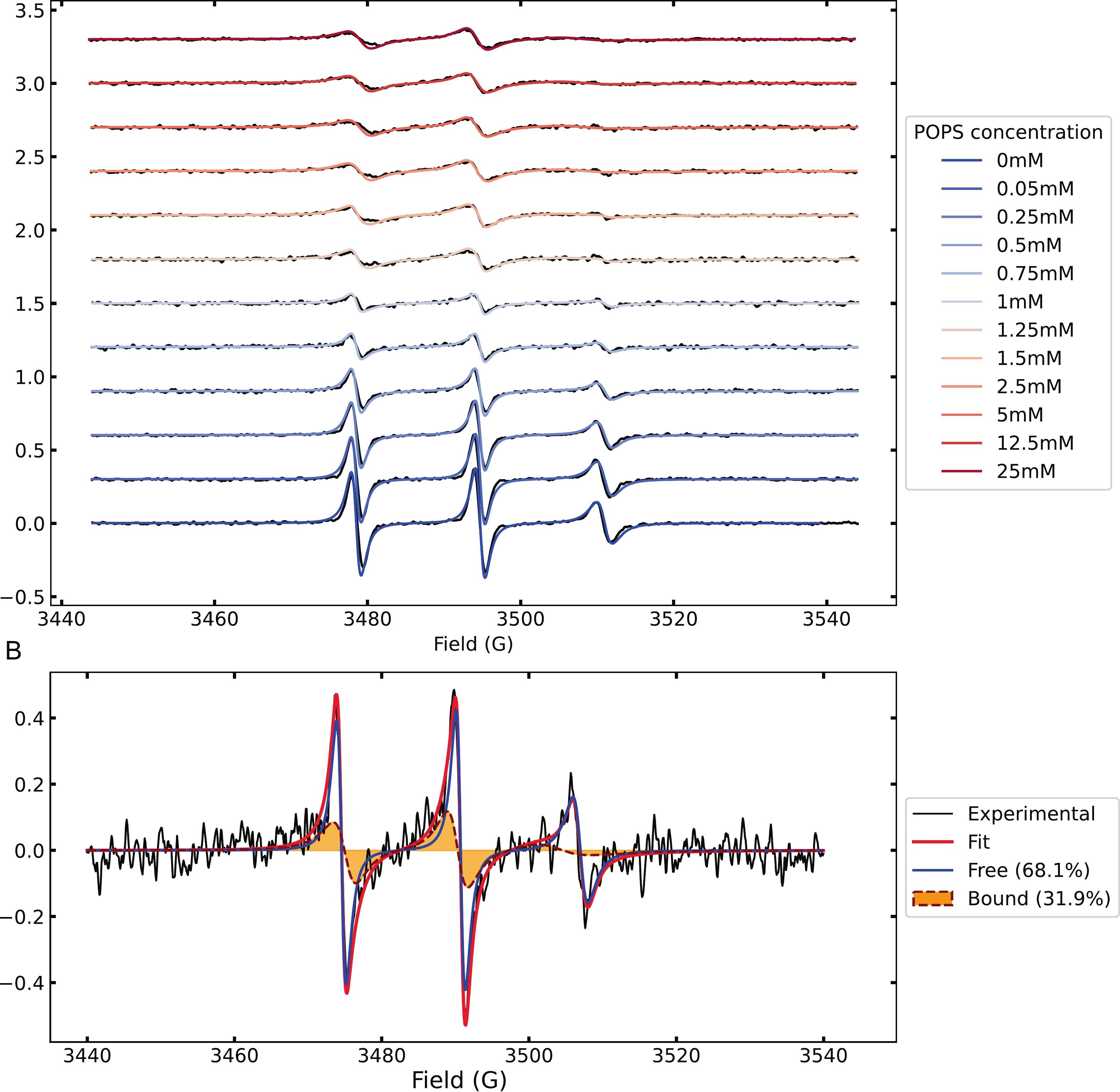
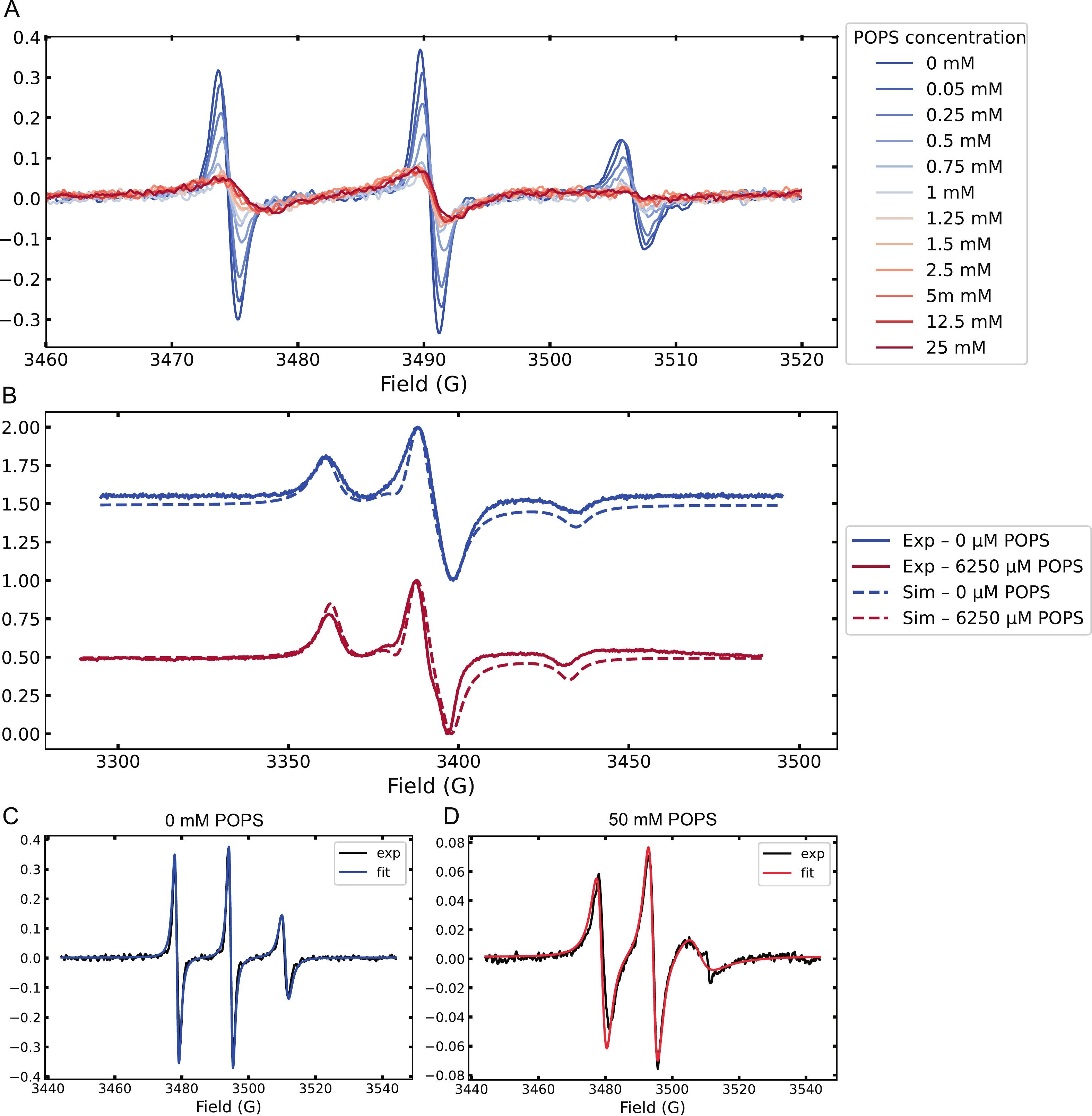 Figure 1. (A) Room-temperature CW-EPR spectra of spin-labeled Tau during titration with increasing concentrations of POPS MLVs, showing gradual line-shape changes.