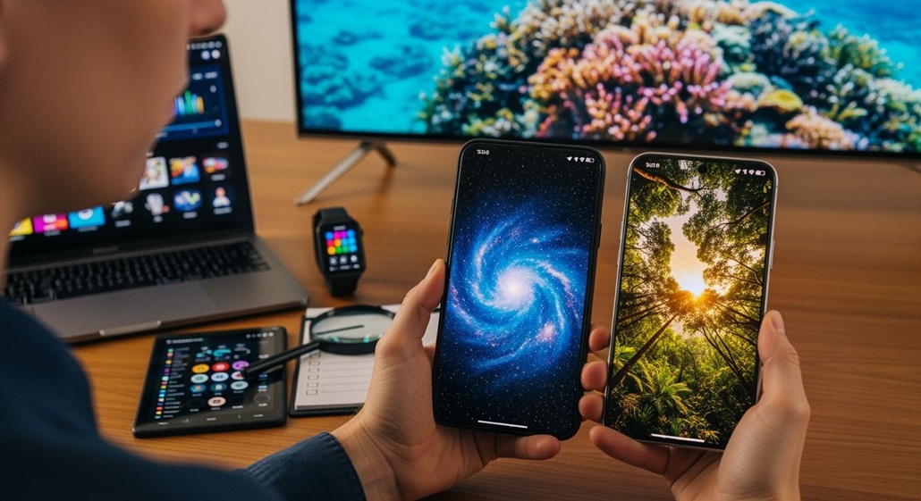
You rely on tft lcd screen technology to overcome visibility challenges in modern electronics. Advanced features such as optimized brightness, improved contrast, and innovative anti-reflective solutions deliver remarkable clarity in tough lighting conditions. The Golden Vision 3.5 Inch IPS lcd module tft display showcases these innovations, offering vibrant colors and wide viewing angles. With high brightness and adaptive lcd module tft solutions, you experience enhanced legibility whether you use consumer or industrial tft lcd displays. The latest lcd module tft advancements ensure every solution meets your expectations for performance and reliability.
|
Feature
|
Impact on Visibility
|
|
High Brightness
|
Improves outdoor readability and legibility
|
|
Optical Bonding
|
Reduces glare and boosts clarity
|
|
IPS Panel Technology
|
Delivers consistent color and image quality from all angles
|
Key Takeaways
-
TFT LCD technology enhances visibility in bright environments with high brightness and anti-reflective features.
-
Sunlight-readable displays improve legibility outdoors, making them ideal for medical monitors and outdoor kiosks.
-
Optical bonding reduces glare and enhances clarity by eliminating air gaps between screen layers.
-
IPS panel technology provides consistent color and image quality from all viewing angles, improving user experience.
-
Adaptive brightness control automatically adjusts screen brightness based on surrounding light, reducing eye strain.
-
Choosing displays with customizable backlight options allows you to balance visibility and energy efficiency.
-
Robust TFT LCD solutions operate reliably in extreme temperatures, ensuring performance in harsh conditions.
-
Selecting the right display involves considering application needs, brightness levels, and durability for optimal performance.
Visibility Challenges for TFT LCD Screens
Modern electronics rely on lcd module tft technology to deliver clear visuals in diverse environments. You encounter several challenges that can impact visibility and readability, especially when using devices outdoors or in demanding settings. Understanding these obstacles helps you choose the right lcd module tft solutions for your needs.
Sunlight and Glare Issues
Outdoor environments present significant hurdles for tft lcd screen performance. Sunlight and glare can dramatically reduce the effective contrast ratio, making images and text nearly unreadable. For example, when sunlight reflects off the display, the contrast ratio may drop from 400:1 to just 2:1. This drastic change means you struggle to see important information on your device. Increasing the brightness or applying anti-reflective coatings can help restore readability and enhance visibility. You benefit from sunlight-readable tft lcd displays in devices like medical monitors, outdoor kiosks, and consumer electronics such as smart coffee machines. These solutions ensure you maintain clear visuals even under direct sunlight.
Tip: Choose lcd module tft displays with high brightness and anti-reflective features for outdoor use. This approach improves readability and reduces eye strain.
|
Challenge
|
Symptoms
|
Causes
|
Solutions
|
|
Backlight Bleeding
|
Light leaks around screen edges
|
Imperfect panel assembly or uneven LED backlight distribution
|
Adjust brightness levels, use local dimming settings, replace panel if excessive
|
|
Uneven Brightness
|
Variations in brightness across the screen
|
Poor manufacturing quality or design flaws
|
Adjust brightness settings, consider panel replacement
|
|
Flickering Screens
|
Noticeable flicker during refresh cycles
|
Faulty driver IC, unstable power supply
|
Update display drivers, stabilize power input, replace faulty components
|
Temperature and Environmental Factors
Environmental conditions play a crucial role in lcd module tft display performance. High humidity can cause electrical malfunctions, corrosion, and fogging, which reduce visibility. Adhesive failures may lead to separation of screen layers, affecting overall performance. Extreme temperatures also pose risks. High temperatures can darken the display, limiting visibility, while low temperatures slow response times and increase power consumption. In some cases, the liquid crystal may freeze, reducing light passage and contrast. You need lcd module tft displays designed for robust operation in harsh conditions to ensure consistent readability.
-
High humidity leads to fogging and reduced visibility.
-
High temperatures cause darkening and limited readability.
-
Low temperatures slow response times and increase power usage.
-
Adhesive failures can separate screen layers, impacting performance.
Viewing Angle Limitations
Viewing angle is another critical factor in enhancing visibility. Poor viewing angles result in color shifting and contrast degradation, making dark scenes hard to discern. You may experience user dissatisfaction, especially when multiple people view the screen at once. In medical settings, accurate and stable visuals are essential for healthcare professionals. A poor viewing angle can lead to misinterpretation, which may affect patient care. Consumer devices also benefit from wide viewing angles, ensuring everyone sees the same clear image regardless of their position.
-
Color shifting occurs at oblique angles.
-
Contrast drops, making details harder to see.
-
Multiple viewers may struggle to interpret information accurately.
You improve user experience and safety by selecting tft lcd displays with wide viewing angles and sunlight-readable tft lcd features. These solutions support enhancing visibility in both consumer and industrial applications.

When you use electronic devices outdoors or in brightly lit environments, you need displays that remain clear and easy to read. Sunlight-readable tft lcd solutions address this challenge by using advanced backlight technology and adaptive brightness features. These innovations ensure that your device delivers excellent readability in sunlight and other high-glare conditions.
High-Brightness Backlight
High brightness is essential for achieving readability in sunlight. Standard tft lcd displays often struggle in outdoor settings because their backlight cannot compete with direct sunlight. You need a display that produces enough high-brightness light to overcome glare and maintain image clarity.
The Golden Vision 3.5 Inch IPS tft lcd display module features a luminance of 350cd/m². While industry standards for daylight-readable liquid crystal displays often start at 800 nits and go up to 1000 nits for true sun readable lcd performance, a 350cd/m² backlight still offers a significant improvement over typical indoor displays. This level of brightness ensures that you can view images and text with greater clarity, even when ambient light is strong.
|
Feature
|
Specification
|
|
Panel Size
|
3.5 Inch
|
|
LCD Type
|
IPS
|
|
Luminance
|
350cd/m²
|
|
View Angle
|
ALL
|
|
Module Size
|
76.9x63.85x2.85 MM
|
|
Display Area
|
70.08x52.56 MM
|
|
Number of Dots
|
640x480
|
You benefit from high-brightness backlight technology in many applications. Medical devices, outdoor kiosks, and industrial controls all require reliable lcd module tft displays that perform well in sunlight. High-brightness solutions help you avoid washed-out screens and ensure that critical information remains visible.
Customizable Backlight Units
Customizable backlight units give you the flexibility to adjust brightness based on your specific needs. The Golden Vision lcd module tft display allows you to tailor the backlight intensity, which helps you balance power consumption and visibility. For portable devices, you can lower the backlight to save energy indoors and increase it for outdoor use. This adaptability makes lcd module tft solutions ideal for a wide range of environments.
-
You can set the backlight to maximum for outdoor readability.
-
You can reduce the backlight indoors to extend battery life.
-
Customizable backlight units support both consumer and industrial applications.
Adaptive Brightness Control
Adaptive brightness control further enhances your experience by automatically adjusting the backlight based on ambient light conditions. Sensors detect the surrounding light and increase the backlight in bright environments or decrease it in low-light settings. This feature ensures that your tft lcd screen always provides optimal readability without manual adjustments.
You gain several advantages from adaptive brightness:
-
Improved readability in sunlight and shade.
-
Reduced eye strain as the display adapts to changing conditions.
-
Consistent performance across different environments.
Sunlight readable solutions, such as those found in the Golden Vision lcd module tft display, combine high-brightness backlight, customizable units, and adaptive brightness control. These features ensure that your device remains visible and user-friendly, whether you use it in direct sunlight or indoors. You can rely on these tft lcd displays for critical applications where visibility matters most.
Note: When you select a tft lcd screen for your project, always consider the brightness rating and backlight options. High-brightness and adaptive features are key to achieving true sunlight readability.
Daylight-readable liquid crystal displays have become essential in modern electronics. You can trust lcd module tft technology to deliver the performance and reliability you need for any environment.

Reduce Reflections and Enhance Clarity
Modern lcd module tft solutions address one of the most persistent challenges in display technology: how to reduce reflections and enhance clarity. When you use a tft lcd screen in bright environments, unwanted reflection can obscure content and reduce readability. Advanced anti-reflective and anti-glare film technologies, along with optical bonding, provide effective ways to reduce reflections and improve the user experience.
Anti-Reflective Coatings
You benefit from anti-reflective coatings because they use sophisticated optical engineering to minimize reflection and glare. These coatings work by manipulating light at the surface of lcd module tft displays, ensuring that more light passes through the screen and less is reflected back at your eyes. This process preserves image quality and enhances clarity, even in challenging lighting conditions.
|
Mechanism
|
Description
|
|
Optical Interference
|
AR coatings use optical interference to reduce mirror-like reflections while preserving image quality.
|
|
Graded-Index Layer
|
A graded-index layer gradually reduces the refractive index, minimizing reflections and enhancing clarity.
|
|
Moth-Eye Structure
|
A nanoscale surface structure that reduces photopic reflectance to less than 0.1%, improving visibility.
|
|
Surface Roughness
|
AG coatings diffuse specular reflections, reducing glare by redistributing reflected light.
|
You see the impact of these coatings in both consumer and industrial applications. For example, medical devices require clear, accurate visuals for critical decisions. Consumer electronics, such as smart appliances, benefit from improved readability in kitchens or outdoor spaces. Anti-reflective and anti-glare film solutions ensure that you experience less eye strain and better clarity, regardless of the environment.
Optical Bonding Technology
Optical bonding technology further enhances lcd module tft displays by physically attaching the cover glass to the display panel with a special adhesive. This process eliminates the air gap that typically exists between layers, which is a major source of internal reflection.
Eliminating Air Gaps
When you remove the air gap, you significantly reduce internal reflection. This leads to sharper images and improved contrast. The content on your lcd module tft display appears more vibrant and legible, even in direct sunlight.
|
Benefit
|
Description
|
|
Reduced Reflections
|
Optical bonding minimizes the reflection and refraction of light, enhancing visibility.
|
|
Improved Clarity
|
Eliminating the air gap leads to sharper, more vibrant images with better contrast.
|
|
Enhanced Visibility
|
Ideal for bright environments, making content clearer and more legible.
|
Improving Durability
Optical bonding not only helps reduce reflections but also increases the durability of your display. The adhesive layer protects the lcd module tft from dust, moisture, and physical impact. This makes it an excellent choice for industrial equipment, outdoor kiosks, and any application where reliability matters.
|
Benefit
|
Description
|
|
Reduced Glare
|
Optical bonding reduces glare, improving visibility in outdoor and well-lit environments.
|
|
Enhanced Contrast
|
The elimination of the air gap enhances contrast, making images and text appear sharper.
|
|
Improved Durability
|
The bonding process increases the durability of the display, protecting it from damage.
|
You gain better legibility, higher clarity, and longer-lasting performance from these advanced technologies. Whether you use tft lcd screens in consumer gadgets or industrial machinery, anti-reflective coatings and optical bonding provide the solutions you need for superior readability and display quality.
Tip: For the best results in high-brightness or outdoor settings, choose lcd module tft displays with both anti-reflective coatings and optical bonding. This combination delivers maximum clarity and reduces reflections for any application.
Modern lcd module tft technology delivers impressive improvements in contrast and color performance. These advancements help you achieve better visibility, sharper images, and more vibrant colors in any environment. When you select the right lcd module tft solution, you ensure your device stands out, even in challenging lighting conditions.
IPS Panel Advantages
You benefit from IPS panel technology because it provides superior viewing angles and color accuracy compared to traditional lcd module tft displays. IPS panels do not show the gray inversion effect, so colors remain consistent from every angle. This feature is essential for applications where multiple users view the screen at once or where precise color reproduction matters.
-
IPS panels maintain color integrity from various angles.
-
The arrangement of liquid crystal molecules in IPS technology allows for better clarity and color accuracy.
-
You avoid the washed-out look and color shifting seen in older tft lcd screens.
|
Feature
|
IPS Panels
|
Traditional TFT Panels
|
|
Viewing Angles
|
Up to 178°
|
Typically around 55°
|
|
Color Reproduction
|
More consistent and stable
|
Colors can shift and appear washed out
|
|
Gray Inversion Effect
|
No gray inversion effect
|
Exhibits gray inversion effect
|
You experience clear information at angles, which is crucial for both driver safety and user experience. This advantage supports eye comfort and reduces visual fatigue during extended use.
Improved Pixel Structure
The structure of each lcd module tft display plays a vital role in delivering high contrast and accurate color. Every component, from the backlight to the color filters, contributes to the overall image quality you see.
|
Component
|
Role in Image Quality
|
|
Backlight
|
Provides illumination for the display
|
|
Polarizing films
|
Control the direction of light
|
|
Glass substrates
|
Contain the liquid crystal material
|
|
Color filters
|
Create red, green, and blue sub-pixels
|
|
TFT array
|
Controls individual pixels
|
|
Liquid crystal layer
|
Alters light transmission based on electrical signals
|
A well-designed pixel structure ensures deeper blacks, brighter whites, and a wide color gamut. You notice images that look more lifelike and text that remains sharp, even in bright environments. Enhanced brightness makes lcd module tft solutions suitable for outdoor use, improving visibility in sunlight.
|
Feature
|
Benefit
|
|
High Contrast Ratios
|
Deeper blacks and brighter whites improve readability in bright environments.
|
|
Wide Color Gamut
|
Ensures images are vibrant and lifelike, enhancing visual feedback.
|
|
Enhanced Brightness
|
Makes displays suitable for outdoor environments, improving visibility in sunlight.
|
Dynamic Contrast Adjustment
Dynamic contrast adjustment gives you the ability to see both bright and dark areas clearly, even when lighting conditions change. This technology uses localized brightness control, so the lcd module tft adapts to your environment in real time.
-
Dynamic contrast adjustment enables localized brightness control, enhancing visibility in varying ambient light conditions.
-
The display renders both bright and dark areas effectively, which is crucial for outdoor visibility.
-
Local dimming zones in advanced backlighting technologies achieve deeper blacks and brighter highlights, improving overall display performance.
You gain a display that responds to your needs, whether you use it indoors or outdoors. These solutions help you maintain high visibility and eye comfort, making tft lcd displays a reliable choice for any application.
Environmental Robustness of TFT LCD Screens
You expect your lcd module tft to perform reliably in a range of environments. Devices often face extreme temperatures, whether in outdoor kiosks, industrial machinery, or medical equipment. Wide temperature lcd solutions ensure that your display remains clear and functional, even when conditions change rapidly. Many specialized tft lcd displays operate from -20°C to +60°C, and some modules reach up to 70°C. Noritake models extend this range from -30°C to 85°C. These wide temperature lcd solutions protect your investment and guarantee consistent performance.
|
Type of Display
|
Operating Temperature Range
|
|
Conventional LCD
|
-10°C to 50°C
|
|
Specialized TFT LCD
|
-20°C to +60°C
|
|
Some Modules
|
Up to 70°C
|
|
Noritake TFT Models
|
-30°C to 85°C
|
You benefit from these robust lcd module tft options in environments where temperature fluctuations could otherwise damage electronics. Wide temperature lcd solutions help you maintain eye comfort and visibility, regardless of the weather or location.
RoHS Compliance and Safety
You want your lcd module tft to meet strict safety and environmental standards. RoHS compliance plays a key role in ensuring that your device is safe for users and the environment. Manufacturers now use eco-friendly materials, replacing lead-based solder with tin-silver-copper alloys. This shift aligns with global regulations such as the EU RoHS Directive. You also see a growing demand for sustainable electronics, and RoHS compliance supports this trend.
|
Key Trends and Drivers
|
Description
|
|
Shift to Eco-Friendly Materials
|
Manufacturers are replacing lead-based solder with tin-silver-copper alloys.
|
|
Global Regulatory Pressure
|
Compliance with regulations like the EU RoHS Directive enhances safety.
|
|
Consumer Preference
|
Demand for sustainable electronics is supported by RoHS compliance.
|
The Golden Vision lcd module tft display module meets RoHS standards, so you can trust its safety and environmental robustness. You protect users and contribute to a healthier planet by choosing RoHS-compliant solutions.
Reliability in Harsh Conditions
You rely on your lcd module tft to deliver stable performance in tough environments. Reliability metrics help you evaluate how well a display will function over time. Stability ensures your device operates without crashes or freezes. Lifespan measures how long your screen remains effective. Anti-interference capabilities protect your display from electromagnetic and electrostatic disruptions. Resistance to high and low temperatures guarantees functionality in extreme conditions.
-
Stability: Your device runs smoothly without interruptions.
-
Lifespan: The screen continues to work effectively for years.
-
Anti-interference capabilities: The display withstands electromagnetic and electrostatic interference.
-
Resistance to high and low temperatures: You get reliable operation in any climate.
You gain peace of mind knowing your lcd module tft can handle demanding environments. These solutions combine durability, safety, and performance, making them ideal for industrial, medical, and consumer applications. High brightness and robust construction further enhance reliability, so you experience clear visuals and eye comfort wherever you use your device.
Eye Comfort and User Experience
You expect lcd module tft screens to deliver consistent comfort and clarity, no matter where you sit or stand. All-view angle technology in modern tft lcd displays ensures that you see uniform brightness, contrast, and color saturation from every direction. This feature eliminates the need to reposition your device, reducing strain and enhancing eye comfort. You experience natural color output and improved readability, which minimizes the factors that influence eye strain. The Golden Vision lcd module tft display integrates all-view angle technology, so you enjoy a comfortable viewing experience whether you use the device alone or share it with others.
|
Feature
|
Benefit
|
|
Consistent image quality
|
Maintains uniform brightness, contrast, and color saturation from various angles.
|
|
Improved color accuracy
|
Eliminates color shifting and loss of contrast, providing a more natural visual output.
|
|
Enhanced readability
|
Reduces eye strain by allowing comfortable viewing without constant adjustments.
|
|
Reduced eye strain
|
Provides a uniform image, minimizing the need for users to reposition their screens.
|
You notice less strain during long periods of use. This technology supports comfort for your eyes and helps you focus on your tasks without distraction.
Touch Panel Options
Touch panel options in lcd module tft screens transform your interaction with devices. You navigate menus, select options, and control functions with simple gestures. Capacitive and resistive touch panels offer intuitive operation, making devices accessible for everyone. Multi-touch capabilities allow you to zoom, scroll, and perform complex actions with ease. These solutions simplify operation and support accessibility features, so individuals with disabilities can use devices comfortably. You no longer need external peripherals, which streamlines your workflow and reduces strain from repetitive movements.
|
Advantage
|
Description
|
|
Intuitive Interaction
|
Touchscreens enable simple gestures like tapping and swiping for easy navigation.
|
|
Multi-Touch Capabilities
|
Allows complex actions such as pinch-to-zoom, enhancing user experience in various applications.
|
|
Accessibility Features
|
Supports assistive technologies, making devices usable for individuals with disabilities.
|
|
Simplified Operation
|
Eliminates the need for external peripherals, making devices easier to use for everyone.
|
You benefit from comfort and reduced strain, especially when using lcd module tft solutions in medical, industrial, or consumer environments.
Energy Efficiency
Energy efficiency plays a vital role in eye comfort and overall user experience. Efficient lcd module tft displays use advanced backlight control and blue light reduction technologies to minimize power consumption and reduce strain. You adjust brightness to suit your environment, which helps lower energy use and supports comfort for your eyes. Blue light reduction features decrease exposure to harmful wavelengths, further reducing strain and supporting long-term eye health. You find these solutions especially valuable in portable devices, where battery life and comfort matter most.
-
Blue light reduction technology lowers exposure to harmful light, decreasing strain.
-
Adaptive brightness settings help you maintain comfort and visibility in any lighting condition.
-
Efficient lcd module tft displays extend battery life and support sustainable device operation.
You experience less strain and greater comfort, whether you use your device for work, study, or leisure. Modern tft lcd displays combine all-view angle technology, touch panel options, and energy efficiency to deliver solutions that prioritize eye comfort and usability.
Choosing the Right TFT LCD Display
Selecting the best lcd module tft for your project requires careful evaluation of specifications, application needs, and cost-performance balance. You want a display that delivers reliability, clarity, and the right features for your environment. The Golden Vision 3.5 Inch IPS module demonstrates how flexibility and advanced technology can meet a wide range of requirements.
Key Specifications to Consider
You should review several key specifications before making a decision. Each factor impacts the performance and suitability of your lcd module tft for different applications. The table below outlines the most important specifications and their descriptions:
|
Specification
|
Description
|
|
Size & Resolution
|
Choose from various sizes and resolutions to fit compact or large devices.
|
|
Viewing Angles & Brightness
|
IPS or MVA technologies improve visibility; sunlight-readable options support outdoor use.
|
|
Touchscreen Requirements
|
Capacitive touch enables multi-touch; resistive touch works well with gloves in industrial settings.
|
|
Interface Compatibility
|
Ensure support for HDMI, EVE, or other interfaces for seamless integration.
|
|
Durability & Lifespan
|
Opt for displays designed for longevity and reliability, especially in demanding environments.
|
You gain the most value by matching these specifications to your project’s needs. The Golden Vision lcd module tft offers customizable options, including touch panel selection and adjustable brightness, making it suitable for both consumer and industrial devices.
Application-Based Selection
Your application determines which lcd module tft features matter most. Follow these steps to ensure you select the right display:
-
Define your requirements:
-
Assess the usage environment. Outdoor devices need higher brightness and wide viewing angles. Indoor devices may prioritize contrast and color accuracy.
-
Identify the display content. Text, images, and videos require different resolutions and color performance.
-
Evaluate display effects:
You should always align your selection with the intended use. For example, medical devices require high accuracy and reliability, while consumer products may focus on vibrant visuals and responsive touch.
Tip: The Golden Vision lcd module tft adapts to various applications, from medical equipment to smart appliances, thanks to its flexible design and robust performance.
Cost vs. Performance
Balancing cost and performance ensures you get the best value from your lcd module tft investment. Consider these points:
-
Industrial displays provide greater reliability and longer lifespan, making them ideal for harsh environments.
-
Consumer displays cost less but suit shorter product cycles and stable conditions.
-
The initial price of an industrial lcd module tft may be higher, but you benefit from lower total ownership costs due to fewer service calls and replacements.
-
Industrial screens use superior materials and robust designs, ensuring consistent performance and durability.
You should weigh the upfront investment against long-term savings and reliability. The Golden Vision module exemplifies a solution that balances advanced features with cost-effectiveness, supporting both demanding and everyday applications.
You solve visibility challenges in modern electronics by choosing lcd module tft solutions that combine sunlight-readable tft lcd, anti-reflective coatings, and high brightness. These technologies deliver clear visuals, reduce glare, and enhance comfort for users. The table below highlights how lcd module tft features improve performance:
|
Technology
|
Benefit
|
|
High Brightness Backlight
|
Increases display brightness for better visibility in sunlight.
|
|
Anti-Reflective Coatings
|
Minimizes reflection and glare, ensuring better readability.
|
You ensure eye comfort and reliability by selecting lcd module tft displays with robust environmental protection. Consider these factors to maximize visibility and comfort in every tft lcd display project.