Latest Electronics News & Trends | Expert Insights & Innovations
scanning electron microscope

CIQTEK SEM Study Shows Raised-Ring Electrodes Improve Aluminum Alloy Spot Welding and Electrode Life

Aluminum alloys, prized for their exceptional strength-to-weight ratio, are ideal materials for automotive lightweighting. Resistance spot welding (RSW) remains the mainstream joining method for automotive body manufacturing. However, the high thermal and electrical conductivity of aluminum, combined with its surface oxide layer, requires welding currents far exceeding those used for steel. This accelerates copper electrode wear, leading to unstable weld quality, frequent electrode maintenance, and increased production costs. Extending electrode life while ensuring weld quality has become a critical technological bottleneck in the industry.


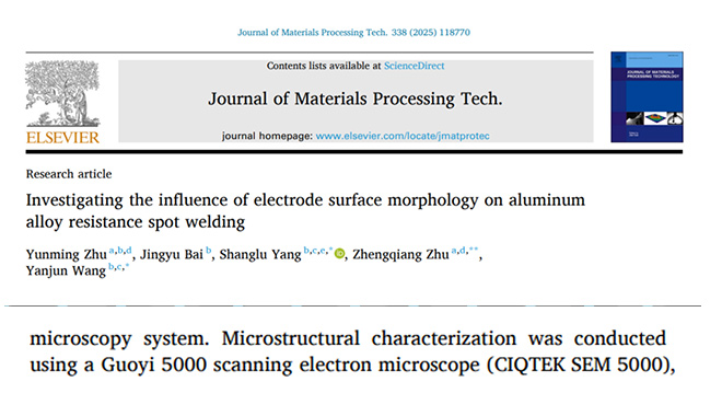
To address this challenge, Dr. Yang Shanglu's team at Shanghai Institute of Optics and Fine Mechanics conducted an in-depth study using the CIQTEK FESEM SEM5000. They innovatively designed a raised-ring electrode and systematically investigated the effect of ring number (0–4) on electrode morphology, revealing the intrinsic relationship between ring count, crystal defects in the weld nugget, and current distribution. Their results show that increasing the number of raised rings optimizes current distribution, improves thermal input efficiency, enlarges the weld nugget, and significantly extends electrode lifespan. Notably, the raised rings enhance oxide layer penetration, improving current flow while reducing pitting corrosion. This innovative electrode design provides a new technical approach for mitigating electrode wear and lays a theoretical and practical foundation for broader application of aluminum alloy RSW in the automotive industry. The study is published in the Journal of Materials Processing Tech. under the title “Investigating the Influence of Electrode Surface Morphology on Aluminum Alloy Resistance Spot Welding.

CIQTEK SEM: Raised-Ring Electrodes Boost Aluminum Welding

Raised-Ring Electrode Design Breakthrough

Facing the electrode wear challenge, the team approached the problem from electrode morphology. They machined 0 to 4 concentric raised rings on the end face of conventional spherical electrodes, forming a novel Newton Ring electrode (NTR).
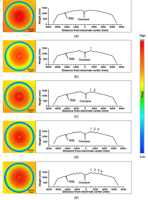
 

Figure 1. Surface morphology and cross-sectional profile of the electrodes used in the experimentFigure 1. Surface morphology and cross-sectional profile of the electrodes used in the experiment


SEM Analysis Reveals Crystal Defects and Performance Enhancement

How do raised rings influence welding performance? Using the CIQTEK FESEM SEM5000 and EBSD techniques, the team characterized the microstructure of weld nuggets in detail. They found that the raised rings pierce the aluminum oxide layer during welding, optimizing current distribution, influencing heat input, and promoting nugget growth. More importantly, the mechanical interaction between raised rings and molten metal significantly increases the density of crystal defects, such as geometrically necessary dislocations (GNDs) and low-angle grain boundaries (LAGBs), within the weld nugget. Optimal performance was observed with three raised rings (NTR3).
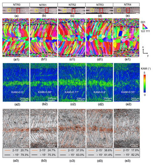
 

Figure 2. EBSD analysis of weld nugget microstructure for NTR0, NTR1, NTR2, NTR3, and NTR4 electrodes

Figure 2. EBSD analysis of weld nugget microstructure for NTR0, NTR1, NTR2, NTR3, and NTR4 electrodes


Prolonged Electrode Life

Beyond improving weld quality, the raised-ring electrodes demonstrate outstanding anti-abrasion performance. After a 10-weld lifespan test, the difference in electrode wear was striking.
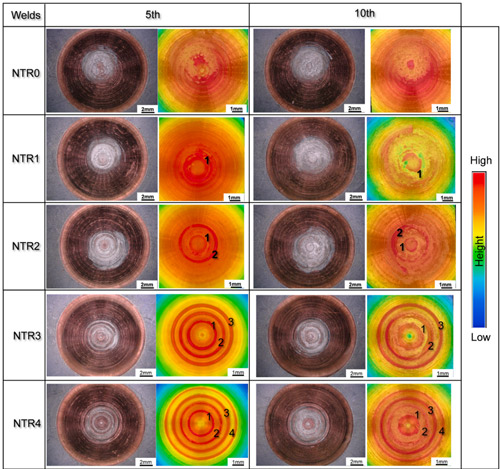
 

Figure 3. Electrode lifespan for NTR0, NTR1, NTR2, NTR3, and NTR4 electrodesFigure 3. Electrode lifespan for NTR0, NTR1, NTR2, NTR3, and NTR4 electrodes


Quantitative Analysis

The NTR0 electrode without raised rings exhibited a wear area of 13.49 million μm².

In comparison, NTR3 and NTR4 electrodes with three and four raised rings reduced wear areas to 4.35 million μm² and 3.98 million μm², representing reductions of 67.8% and 70.5%, respectively.

The raised-ring structure concentrates current along the rings, guiding wear along predetermined paths and preventing random pit expansion, effectively doubling electrode lifespan.
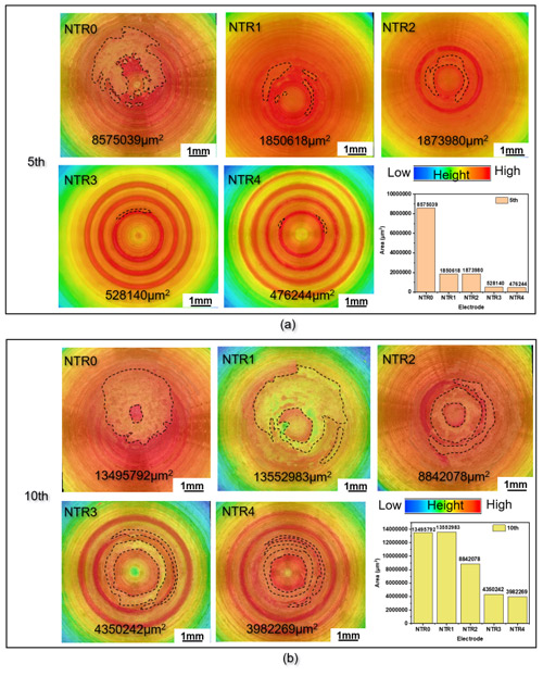
 

Figure 4. Pitting area of NTR0, NTR1, NTR2, NTR3, and NTR4 electrodes after 5 and 10 welds: (a) 5th weld, (b) 10th weldFigure 4. Pitting area of NTR0, NTR1, NTR2, NTR3, and NTR4 electrodes after 5 and 10 welds: (a) 5th weld, (b) 10th weld、


Microanalysis of Electrode Pitting

Further SEM analysis of NTR0 electrodes after welding until adhesion to the aluminum sheet revealed a 10 μm-thick intermetallic compound (IMC) layer between the electrode and the sheet. This transition layer consists of two copper-containing sublayers:

Near the electrode: thinner sublayer with 29.2 at.% Cu (Al4Cu9 phase).

Near the aluminum alloy: thicker sublayer with 15.5 at.% Cu (AlCu2 phase).


Figure 5. Composition analysis of pitting between the electrode and the sheetFigure 5. Composition analysis of pitting between the electrode and the sheet


This study demonstrates that innovative electrode morphology can effectively regulate current distribution, improving weld quality while extending electrode life. CIQTEK FESEM microscope provided indispensable visualization and quantitative evidence of microscopic mechanisms, including crystal defect evolution and electrode pitting, highlighting the critical role of advanced characterization in advancing welding research and industrial applications.

阅读全文......

CIQTEK Launches 12-inch Wafer Inspection Solution for Non-Destructive, High-Resolution Full-Coverage Analysis

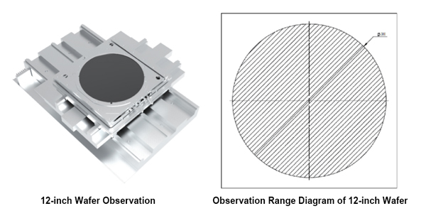
CIQTEK has introduced its next-generation 12-inch wafer scanning electron microscope (SEM) solution, designed to meet the demands of advanced semiconductor manufacturing processes. Offering full-wafer inspection without the need for rotation or tilting, this innovative solution ensures high-resolution, non-destructive analysis to support critical process development.

Equipped with an ultra-large travel stage (X/Y ≥ 300 mm), the system provides complete coverage of 12-inch wafers, eliminating the need for sample cutting or transfer. This ensures true "original size, original position" observation. With a Schottky field emission electron gun, it achieves a resolution of 1.0 nm at 15 kV and 1.5 nm at 1 kV, minimizing electron beam damage, making it ideal for sensitive materials and structures.


CIQTEK 12-inch Wafer SEM for High-Resolution Inspection


Key features include:

  • Ultra-large travel stage (X/Y > 300 mm) for full-wafer inspection

  • High-resolution imaging: 1.0 nm at 15 kV and 1.5 nm at 1 kV

  • Automated loading and optical navigation system for fast wafer exchange and precise positioning

  • Intelligent software for auto-focus, astigmatism correction, and multi-format image output


CIQTEK's 12-inch wafer inspection SEM is more than just an observation tool; it's a critical instrument driving higher yields and smaller nodes in semiconductor manufacturing.


September 26–30, Wuhan
CIQTEK will unveil eight cutting-edge electron microscopy solutions at the 2025 Chinese National Conference on Electron Microscopy!

阅读全文......

CIQTEK to Exhibit at MC2025 Microscopy Conference in Karlsruhe, Germany

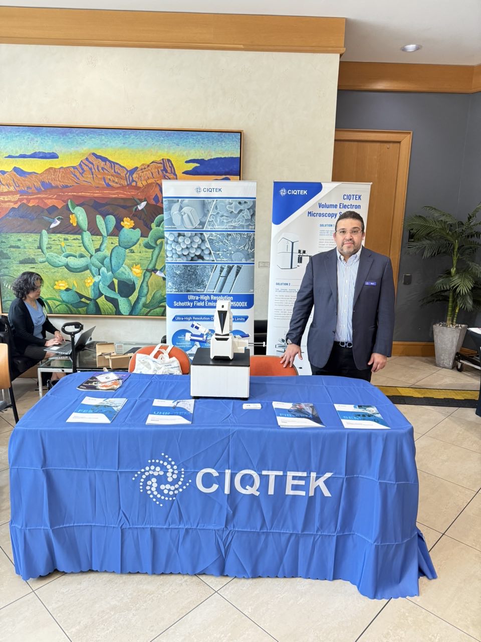
CIQTEK is pleased to announce its participation in the Microscopy Conference 2025 (MC2025), taking place August 31 – September 4 in Karlsruhe, Germany.

You can find us at Booth #28 in the exhibition area of Messe Karlsruhe.


MC2025 is one of the most important events in the international microscopy community, jointly organized by the German Society for Electron Microscopy (DGE), the Austrian Society for Electron Microscopy (ASEM), and the Swiss Society for Optics and Microscopy (SSOM), under the patronage of the European Microscopy Society (EMS). The conference brings together scientists, engineers, and industry leaders to share the latest advances in imaging technologies, applications, and techniques.


Exhibitor Presentation

Date & Time: Monday, September 1st, 17:10 – 17:20 pm
Location: Conference Hall, Messe Karlsruhe
Topic: Unlocking the Power of High-Speed Scanning Electron Microscopy Without Compromising Superb Imaging Resolution at Low kV

During this session, our Senior Electron Microscopy Engineer will share insights into how CIQTEK’s latest high-speed SEM technology achieves exceptional imaging resolution at low accelerating voltages, enabling breakthroughs in materials science, life sciences, and nanotechnology research.


We look forward to connecting with researchers, partners, and industry peers at MC2025. Visit Booth #28 to explore our advanced electron microscopy solutions and discuss how CIQTEK can support your work.


See you in Karlsruhe!

CIQTEK to Exhibit at MC2025 Microscopy Conference in Karlsruhe, Germany

阅读全文......

USTC Team《AM》 | CIQTEK SEM Assists in The Microscopic Morphology Analysis of Potassium Metal Anode


Professor Yan Yu's team at USTC utilized the CIQTEK Scanning Electron Microscope SEM3200 to study the post-cycling morphology. It developed amorphous carbon with controllable defects as a candidate material for an artificial interface layer balancing potassiophilicity and catalytic activity.


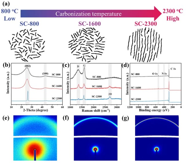
The research team prepared a series of carbon materials with different degrees of defects (designated as SC-X, where X represents the carbonization temperature) by regulating the carbonization temperature. The study found that SC-800 with excessive defects caused substantial electrolyte decomposition, resulting in an uneven SEI film and shortened cycle life. SC-2300, with the fewest defects, had insufficient affinity for potassium and easily induced potassium dendritic growth. SC-1600, which possessed a locally ordered carbon layer, exhibited an optimized defect structure, achieving the best balance between potassiophilicity and catalytic activity. It could regulate the electrolyte decomposition and form a dense and uniform SEI film.


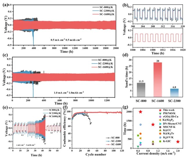
The experimental results demonstrated that SC-1600@K exhibited long-term cycle stability for up to 2000 hours under a current density of 0.5 mA cm-2 and a capacity of 0.5 mAh cm-2. Even under higher current density (1 mA cm-2) and capacity (1 mAh cm-2), it maintained excellent electrochemical performance with stable cycles exceeding 1300 hours. In full-cell testing, when paired with a PTCDA positive electrode, it maintained 78% capacity retention after 1500 cycles at a current density of 1 A/g, demonstrating outstanding cycle stability.


This research, titled "Balancing Potassiophilicity and Catalytic Activity of Artificial Interface Layer for Dendrite-Free Sodium/Potassium Metal Batteries," was published in Advanced Materials.

Figure 1: The microstructure analysis results of carbon samples (SC-800, SC-1600, and SC-2300) prepared at different carbonization temperatures are presented. Through techniques such as X-ray diffraction (XRD), Raman spectroscopy, X-ray photoelectron spectroscopy (XPS), and wide-angle X-ray scattering (WAXS), the crystal structure, defect level, and oxygen and nitrogen doping of these samples were analyzed. The results showed that as the carbonization temperature increased, the defects in the carbon materials gradually decreased, and the crystal structure became more orderly.


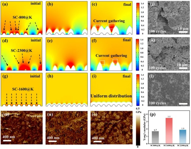
Figure 2: The current density distribution during potassium metal growth on different composite negative electrodes was analyzed using finite element simulation. The simulation results showed that the SC-1600@K composite electrode exhibited a uniform current distribution during potassium deposition, which helped suppress dendritic growth effectively. Additionally, the Young's modulus of the SEI layer was measured using atomic force microscopy (AFM), and the results showed that the SEI layer on the SC-1600@K electrode had a higher modulus, indicating its stronger firmness and inhibition of dendritic formation.


Figure 3: The electrochemical performance of different composite electrodes (SC-800@K, SC-1600@K, and SC-2300@K) in symmetrical cells is presented. The SC-1600@K electrode exhibited excellent cycle stability and low overpotential at different current densities and capacities. Furthermore, electrochemical impedance spectroscopy (EIS) and Sand's time testing further confirmed the advantages of the SC-1600@K electrode in suppressing dendritic growth and maintaining SEI layer stability.


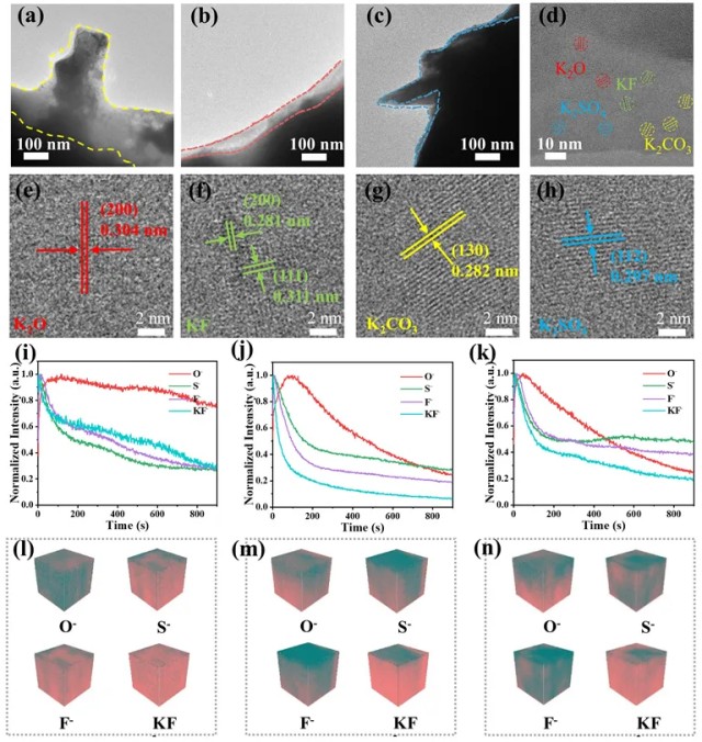
Figure 4: The structure and composition of the SEI layer on different composite negative electrodes were analyzed using cryogenic transmission electron microscopy (Cryo-TEM) and time-of-flight secondary ion mass spectrometry (ToF-SIMS). The results showed that the SC-1600@K electrode had a uniform, thin, and inorganic-rich SEI layer, facilitating fast potassium ion transport kinetics and high Young's modulus. The SEI layers on the SC-800@K and SC-2300@K electrodes exhibited thicker and organic-rich characteristics.


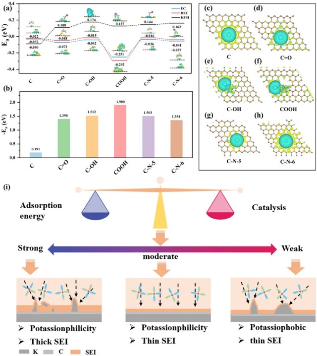
Figure 5: The effects of defect configuration in the carbon layer on potassium ion deposition and SEI formation were explored using density functional theory (DFT) calculations. The results showed that an appropriate amount of defects could enhance the interaction between potassium ions and the carbon layer, reducing the nucleation overpotential, while excessive defects could lead to excessive electrolyte decomposition.


Figure 6: The electrochemical performance of a full cell (PTCDA//SC-1600@K) assembled using the SC-1600@K electrode is presented. This cell exhibited excellent rate performance and long-term cycle stability at different current densities, demonstrating the potential of the SC-1600@K electrode in practical battery applications.


In conclusion, the research team successfully designed and prepared a carbon material (SC-1600) with a locally ordered structure, serving as an artificial interface layer for sodium/potassium metal battery negative electrodes. By precisely controlling the defect content of the material, the team achieved the optimal balance between potassiophilicity and catalytic activity, significantly improving the uniform deposition of potassium ions and promoting the formation of a stable SEI layer. In a potassium symmetrical cell based on SC-1600 in a carbonate electrolyte system, SC-1600@K exhibited excellent cycle stability with a cycle life exceeding 2000 hours. Notably, a full cell assembled with the SC-1600@K negative electrode and PTCDA positive electrode maintained 78% capacity retention after 1500 cycles at a high current density of 1 A/g. This research not only established a model system for optimizing the SEI structure and potassium ion adsorption by controlling the interfacial layer defects but also provided important theoretical guidance and a technological pathway for the rational design of protective interfacial layers in potassium metal batteries.

阅读全文......