Key Findings and Value at a Glance
Understanding how intrinsically disordered proteins interact with biological membranes is a long-standing challenge in biophysics. In a recent study published in Biophysical Chemistry (2026, 329:107550), Dr. Yann Fichou and his team at the University of Bordeaux, France, developed a robust quantitative EPR spectroscopy method to directly measure Tau protein–lipid interactions. Their approach does not rely on indirect probes or relative fluorescence signals, enabling precise, absolute quantification of both free and membrane-bound protein populations.
Using the CIQTEK EPR200M benchtop X-band EPR spectrometer, the team quantitatively resolved the binding behavior of Tau protein to negatively charged lipid membranes, extracted absolute concentrations of free and bound protein populations, and determined binding affinity with minimal experimental input. This work not only reveals key mechanistic insights into Tau–membrane interactions, but also demonstrates the power of CW EPR for quantitative analysis in complex biological systems.
Background: Why Quantifying Protein–Lipid Interactions Is So Difficult
Protein–lipid interactions play a central role in cellular signaling, membrane organization, and the aggregation of pathological proteins. In neurodegenerative diseases such as Alzheimer’s disease, the interaction between Tau protein and cellular membranes is believed to be a critical early event that triggers pathological aggregation.
Despite its importance, quantitative characterization of these interactions remains challenging. Biological membranes are heterogeneous, dynamic, and highly sensitive to experimental conditions. The interactions themselves are often weak, transient, and involve multiple conformational states. Conventional methods such as fluorescence or colorimetric assays typically provide relative signals and require calibration curves that introduce additional uncertainty.
EPR spectroscopy offers a fundamentally different approach. By directly probing the dynamics of spin-labeled molecules, quantitative EPR provides a sensitive and accurate window into molecular motion, binding, and conformational restriction, enabling precise determination of protein–lipid interactions.
From Spectral Line Shapes to Molecular Binding Dynamics
Tau is an intrinsically disordered protein, and its interaction with lipid membranes involves subtle changes in molecular mobility rather than large structural rearrangements. This makes CW EPR particularly well suited to the problem.
Tau protein was site-specifically labeled using site-directed spin labeling (SDSL). Continuous-wave EPR spectra were acquired on the CIQTEK EPR200M at room temperature and 150 K while increasing the concentration of POPS multilamellar vesicles (MLVs).
Free Tau shows a narrow, symmetric three-line spectrum corresponding to rapid isotropic motion (τc ≈ 0.383 ns), characteristic of intrinsically disordered proteins. As POPS concentration increases, spectral broadening and longer rotational correlation times (up to 2.25 ns) indicate progressive restriction of Tau motion upon membrane binding.
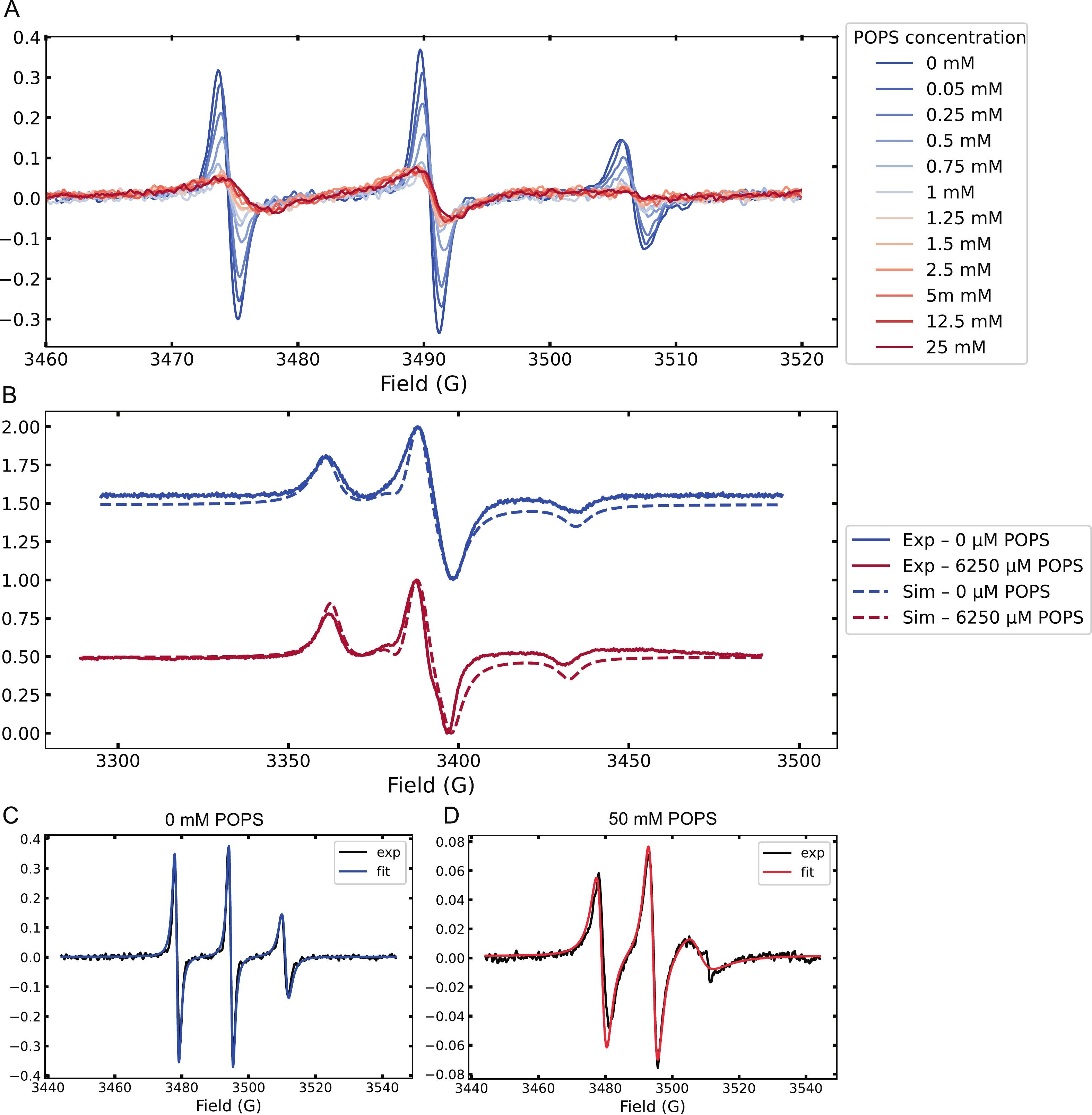 Figure 1. (A) Room-temperature CW-EPR spectra of spin-labeled Tau during titration with increasing concentrations of POPS MLVs, showing gradual line-shape changes.
(B) Frozen-state (150 K) EPR spectra and simulations of spin-labeled Tau in the absence (blue) and presence (red) of 25 mM POPS MLVs.
(C) Room-temperature EPR spectrum of Tau monomers in a free environment.
(D) Room-temperature EPR spectrum of Tau monomers in a restricted environment. Tau concentration was 50 μM. The free environment corresponds to Tau in buffer, while the restricted environment corresponds to Tau in solution containing MLVs.
Absolute Quantification via Two-Component Spectral Deconvolution
A key breakthrough of this work is the use of EPR signal intensity for absolute quantification. Signal intensity is directly proportional to the number of unpaired electrons, allowing precise determination of free and bound protein concentrations without calibration standards.
Using the high baseline stability and signal-to-noise ratio of the CIQTEK EPR200M, experimental spectra were linearly decomposed into free and membrane-bound components. This two-component deconvolution enables calculation of absolute protein concentrations, providing a solid foundation for constructing Hill-type binding models and determining apparent dissociation constants (K_D).
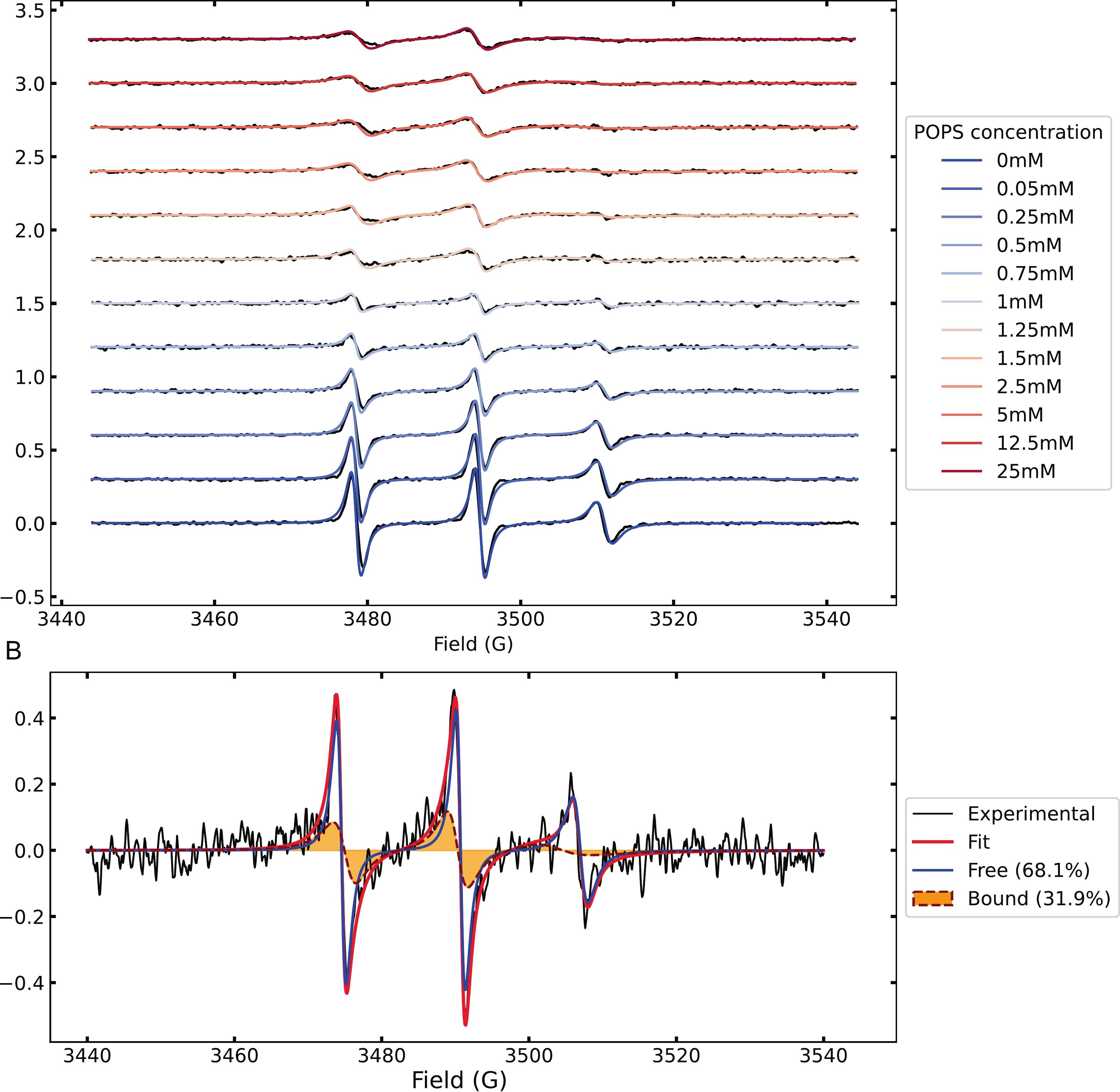 Figure 2. (A) Experimental EPR spectra of spin-labeled Tau at different POPS concentrations (black) and corresponding best-fit simulations (blue to red).
(B) Example of spectral decomposition into free (blue) and bound (orange filled) components.
Minimalist Strategy for Rapid and Accurate Affinity Determination
Error propagation analysis identified optimal conditions for accurate K_D determination: when approximately half of the Tau population is bound (θ ≈ 0.4–0.6), experimental uncertainty is minimized. A single EPR measurement using the EPR200M suffices to obtain apparent dissociation constants matching full titration results, reducing both experimental time and precious sample consumption.
Reliable Performance Trusted by International Users
The CIQTEK EPR200M demonstrates stable microwave performance, sensitive detection, and reliable room-temperature operation. These features support reproducible data acquisition for complex biological samples, from room-temperature dynamics to low-temperature hyperfine analysis.
The successful application at the University of Bordeaux confirms that CIQTEK instruments provide robust support for frontier life science research in Europe and globally.
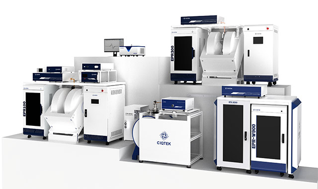
CIQTEK EPR Solutions for Quantitative Research
CIQTEK offers a comprehensive range of EPR instruments:
-
X-band CW & pulsed systems: benchtop or floor-standing, compatible with variable temperature, light, electrochemistry, and in situ modules.
-
High-field Q- and W-band systems: higher magnetic fields and spectral resolution for materials, quantum states, and advanced biophysical studies.
With proven performance, CIQTEK EPR instruments are installed across Europe, North America, and Asia, supporting hundreds of research labs and industrial partners worldwide.