Following the successful delivery of the first phase of 10 Outdoor LED Billboards in the first half of this year, CNLC has once again shipped a new batch of 10 Outdoor LED Billboards (7.5m × 1.92m) to Central Asia.This marks another milestone in our continuous effort to support smart city street advertising projects with reliable and visually stunning display solutions.
Soon, these LED billboards will stand proudly along major city roads, becoming vibrant platforms for urban information sharing and digital outdoor advertising.As trucks rolled out from our factory, each billboard represented more than technology — it carried CNLC’s dedication to quality, innovation, and performance.
Smart Engineering for Smarter Cities
Every CNLC billboard embodies precision engineering and field-tested reliability. Equipped with P5 High Visor LED modules, each display delivers exceptional clarity and contrast, ensuring brilliant performance even under direct sunlight. With 6500nits high brightness, content remains sharp and engaging throughout the day and night.
The aluminum structure provides excellent durability and anti-corrosion protection, making it ideal for long-term outdoor use. An IP56 weatherproof rating shields the display from rain, dust, and temperature fluctuations, while the intelligent temperature control system and air duct cooling design maintain stable operation under all conditions.
Every design choice reflects CNLC’s pursuit of long-lasting performance and visual excellence in every project we deliver.
Every Shipment Tells a Story of Precision and Passion
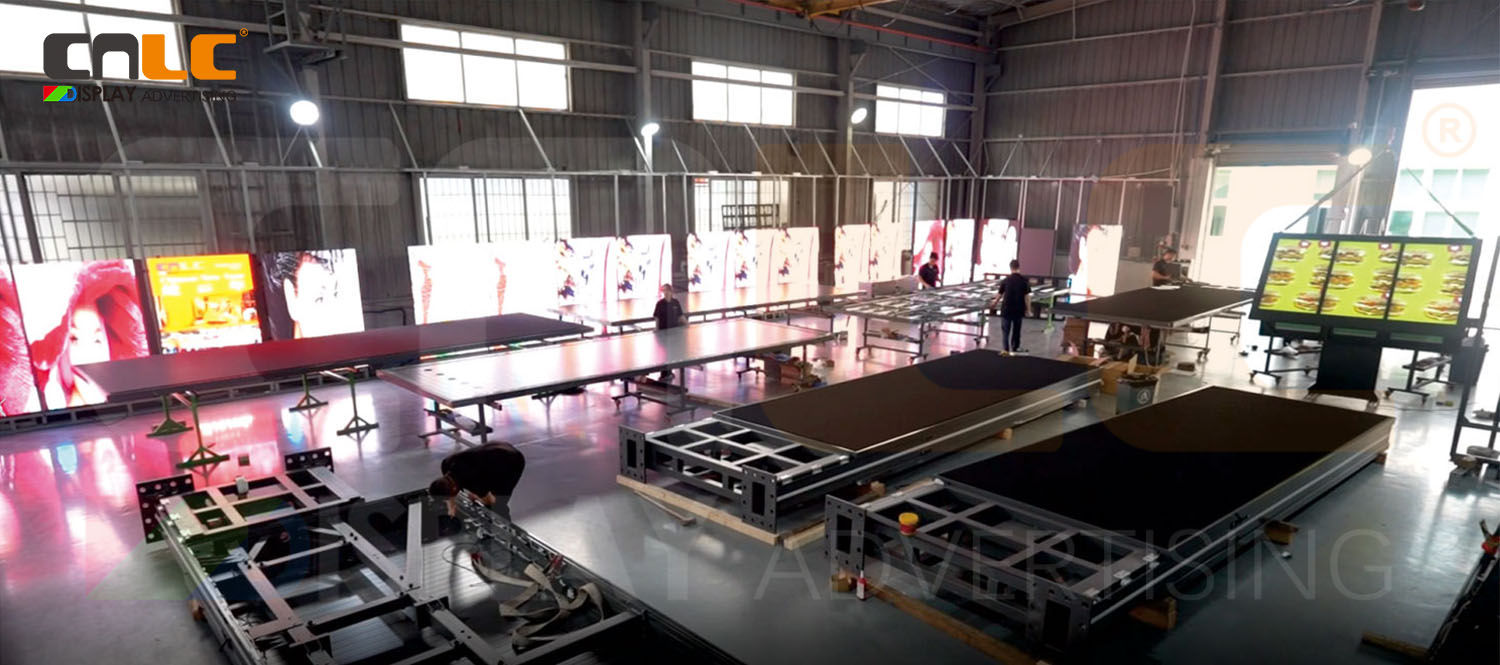
Before leaving the factory, every billboard undergoes strict quality inspections and a 72-hour aging test to ensure optimal stability and image performance.Once approved, the billboards are carefully packed with 10cm protective foam, securing every detail for long-distance transport.
Each truck’s departure marks a moment of pride — a symbol of CNLC’s craftsmanship and our ongoing mission to illuminate cities through intelligent digital displays.
Lighting Up Central Asia and Beyond
With each shipment, CNLC continues to expand its footprint across Asia and Europe, providing high-brightness LED display solutions that bring cities to life.These new installations in Central Asia are another step forward in creating smarter, brighter, and more connected urban environments.
Brighter cities. Smarter connections. CNLC — your trusted partner in outdoor display technology.
According to Statista, the global Digital Out-of-Home (DOOH) advertising market is expected to reach USD 33 billion by 2025, with fuel stations becoming one of the most rapidly expanding segments. This transformation is driven by the growing demand for dynamic, high-visibility, and remotely managed advertising solutions.
🔹 Digital Transformation in the Fuel Industry
As competition intensifies in the energy and retail sectors, gas stations are accelerating their digital transformation. Traditional posters and backlit signs are being replaced by high-definition LED displays that deliver flexibility, efficiency, and vivid visuals.
Studies show that an average customer spends 3–5 minutes at a fuel station — offering a valuable window for impactful advertising exposure. Digital LED billboards not only modernize the station’s image but also create new profit opportunities through third-party advertising.
🔹 Why Outdoor LED Billboards Are Ideal for Gas Stations
Gas stations face constant exposure to sunlight, rain, dust, and temperature fluctuations — demanding displays that remain stable and visible in all conditions.
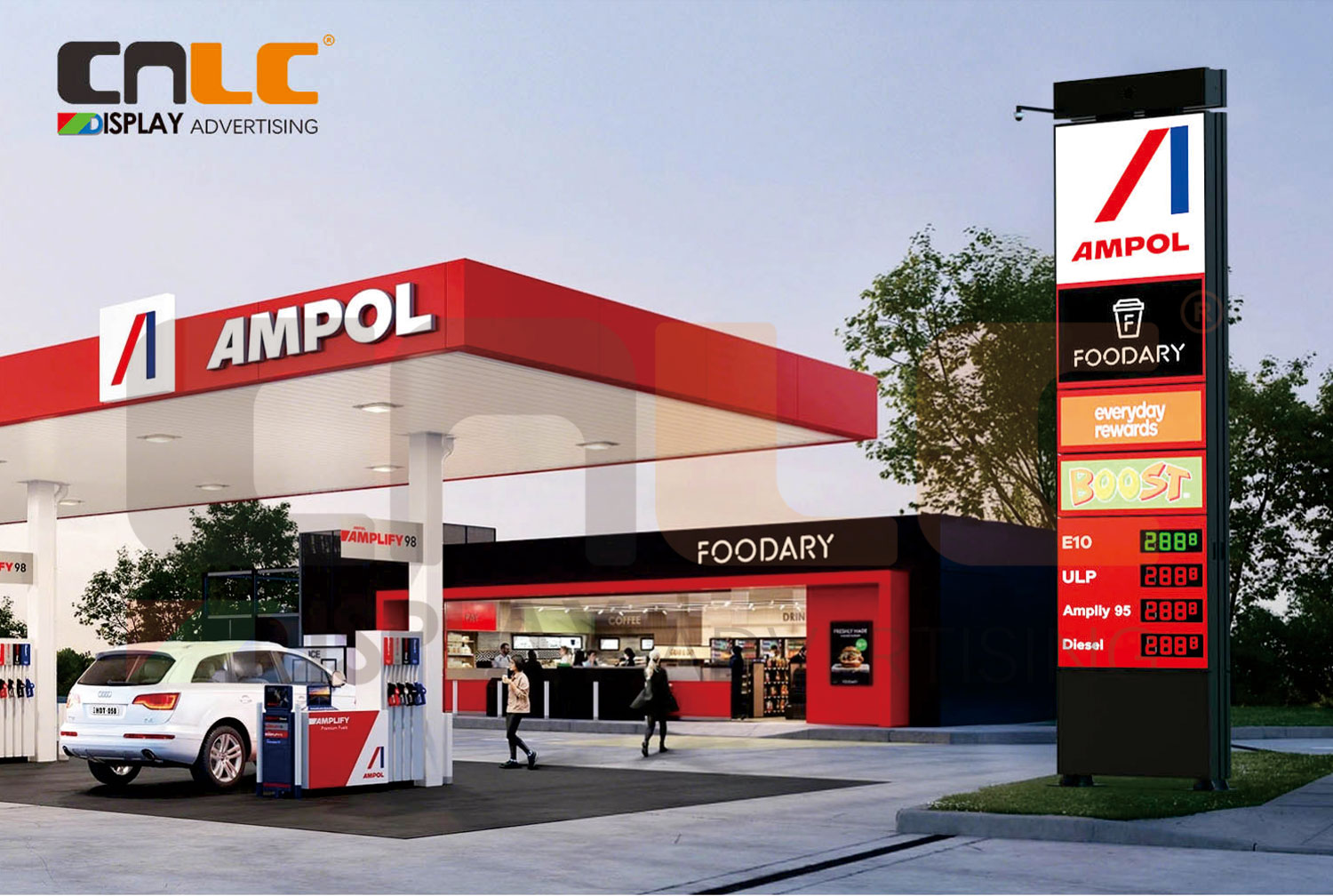
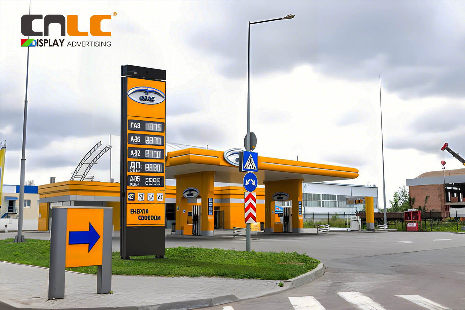
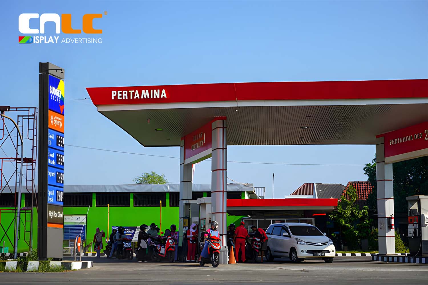
That’s why high-brightness LED billboards have become the preferred choice. With brightness levels exceeding 5000 nits, they maintain perfect visibility even under 100,000 lux of direct sunlight — up to five times brighter than traditional LCD displays. Drivers can easily view fuel prices, promotional content, and safety messages, even from a distance or under strong daylight.
🔹 Performance Meets Durability
Modern LED billboard systems are designed for both outstanding visuals and long-term reliability.
For example, CNLC’s outdoor LED billboard for gas stations features a P5 high-visor LED module with a dual-layer shading design, effectively reducing glare while maintaining high con
trast and vivid colors.
Its precision-engineered aluminum structure provides excellent heat dissipation and corrosion resistance. With an IP56 weatherproof rating, the display ensures stable 24/7 operation under rain, dust, or extreme temperatures — ideal for outdoor environments.
🔹 Smart Control and Efficient Operation
One of the biggest advantages of digital LED signage is remote content management. Operators can instantly update fuel prices, upload new videos, or schedule campaigns across multiple locations — all from a central control system.
This not only minimizes manual maintenance but also ensures that marketing messages stay consistent, accurate, and timely, allowing gas station owners to manage their networks more efficiently.
🔹 Energy Efficiency and Sustainability
Beyond performance, energy efficiency plays a crucial role in today’s outdoor displays.CNLC adopts common cathode energy-saving LED module solutions, delivering superior brightness with significantly reduced power consumption — less than 130W/㎡ while maintaining over 6000 nits of brightness.
In addition, the system integrates intelligent brightness adjustment, automatically adapting to ambient light conditions to further lower energy usage and extend component lifespan.
For example, in our outdoor LED billboard project in Astana, the screen measures 9×6 meters and achieves 6500 nits of brightness using this energy-saving configuration.With the support of CNLC’s intelligent brightness control system, the average daily power consumption is approximately 95 kWh, ensuring both visual impact and sustainable operation.
This balance between performance and energy conservation allows CNLC displays to reduce operating costs while supporting green, eco-friendly advertising — aligning perfectly with the global trend toward sustainable digital signage.Compared with conventional LED billboards, CNLC’s common cathode system reduces energy consumption by up to 30%, while maintaining consistent brightness and long-term reliability.
🔹 Enhancing Customer Experience
Outdoor LED billboards are more than advertising tools — they elevate the customer experience. Dynamic content such as weather forecasts, safety messages, or real-time promotions keeps customers informed and entertained during refueling. This transforms a routine stop into an engaging and value-driven moment, reinforcing brand awareness and boosting in-store sales.
🔹 Conclusion
As the fuel retail industry evolves toward smarter and more connected operations, outdoor LED billboards are becoming an integral part of modern gas station design. Combining high brightness, durable aluminum housing, IP56 protection, and remote content management, they deliver reliability and impact in any environment.
With over 18 years of manufacturing experience and more than 1,000 successful global installations, CNLC continues to lead in providing high-performance, energy-efficient outdoor digital signage solutions trusted by clients worldwide.
💡 For fuel stations looking to modernize their image and maximize advertising value, CNLC’s outdoor LED billboard offers a future-ready and cost-effective solution.
1. Proven Reliability Through 18 Years of Innovation
Since its founding in 2007, CNLC has specialized in the development of outdoor LED and LCD advertising displays, with successful installations across Europe, the Middle East, Asia, and North America.
Our engineering team focuses on one mission — ensuring every display performs flawlessly in any environment.
All CNLC outdoor products are designed, simulated, and tested to meet the highest industrial standards, including IP56/IP65/IP66 waterproofing, IK10 impact resistance, and operational stability under extreme heat.
2. IP65 Waterproof Display with IP56 & IP66 Options for All Outdoor Environments
Outdoor environments are unpredictable — from sandstorms to heavy rainfall. CNLC’s displays achieve IP56, IP65, and IP66 protection levels through:
Precision-engineered sealing structures
High-elastic silicone gaskets
Waterproof connectors and drainage systems
Anti-corrosion aluminum profiles
🔹 IP65 Definition:
The first digit “6” represents complete dust protection, while the second digit “5” ensures resistance against low-pressure water jets from any direction — a balance between accessibility and full weather resistance.
This level of protection guarantees stable operation in coastal, humid, and high-rainfall regions, making CNLC’s outdoor screens ideal for public billboards, city displays, and transportation hubs.
3. Thermal Simulation & Cooling System Excellence
Beyond waterproofing, thermal stability is crucial for long-term display performance. CNLC validates every design through thermal simulation under harsh conditions — 1480 W full power and 800 W/m² solar irradiance, with ambient temperatures reaching 35 °C.
Simulation Parameters
Parameter
Value
Condition
Maximum Power Consumption
1480 W
Full load operation
Solar Irradiance
800 W/m²
Simulated peak sunlight
Ambient Temperature
35 °C
Outdoor standard
Internal Airflow Velocity
2.3 m/s
Simulated convection
Aluminum Thermal Conductivity
205 W/m·K
6063-T5 Aluminum Alloy
Results show a uniform temperature distribution between 39 °C and 71 °C, confirming that CNLC’s enclosure design effectively prevents overheating — even under continuous operation.
This precision is achieved through CNLC’s integrated cooling architecture:
Bottom air intake with dust filters
Upward airflow & top-mounted exhaust fans
Front-facing air ducts for direct heat extraction from the display surface
Smart temperature control system for adaptive fan speed and low noise
4. Aluminum Structure & Optical Protection
All CNLC enclosures are built using 6063-T5 aluminum alloy, featuring a thermal conductivity of 205 W/m·K and excellent corrosion resistance. This material not only ensures efficient heat transfer but also offers lightweight strength for easier installation and maintenance.
In addition, CNLC integrates 6–8 mm tempered laminated glass with optional IR filtering to block heat and UV radiation while maintaining over 75% visible light transmission — delivering vivid image clarity and durability.
5. Trusted Worldwide — Tailored for Your Needs
From gas stations to transportation hubs and urban billboards, CNLC displays are trusted by partners across Europe, Asia, and North America.
Each solution can be customized by:
IP Rating (IP56 / IP65 / IP66)
Cooling System (Air-cooled / A/C-assisted)
Screen Size & Brightness
Glass Type (Standard / IR-filtered)
Mounting & Structural Design
Our global clients choose CNLC not just for our products, but for our commitment to quality, precision, and long-term reliability.
Experience Precision. Experience CNLC.
Whether you need a high-brightness LED billboard, a smart city digital signage solution, or a fully customized outdoor display system — CNLC delivers performance you can trust.
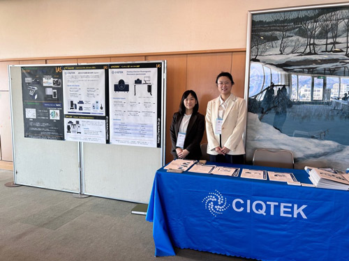
During SEST 2025, many researchers visited the booth to learn about CIQTEK’s technical advantages, such as precise magnetic field control, stable microwave frequency performance, flexible variable-temperature configurations, and advanced pulse sequence capabilities. The event provided an opportunity for in-depth discussions on experimental workflows and potential collaborations.
CIQTEK has established a strong global presence in the EPR field. More than 200 EPR spectrometers have been delivered to research institutions across Asia, Europe, the Americas, etc. The instruments have supported the publication of over 170 scientific papers, including studies featured in Nature, Science, and other leading journals. This growing body of research demonstrates the reliability and scientific value of CIQTEK’s EPR technology.
CIQTEK will continue strengthening its partnership with LASystems to bring high-performance EPR solutions and localized support to researchers throughout Japan.
This blog will explore how different magnetic core materials impact inductor performance, why choosing the right material is critical, and how these materials affect the efficiency and longevity of your electronic devices.
The Importance of Magnetic Core Material
Magnetic cores play a vital role in the function of inductors. They influence inductance, energy storage, efficiency, and power losses. The performance of an inductor is highly dependent on the magnetic material it’s made from, and the right choice of material can make a significant difference in how well the device operates across different frequencies and power levels.
There are several materials commonly used for magnetic cores in inductors, such as ferrite, silicon steel, and nanocrystalline alloys. Each material comes with its own set of advantages and limitations, making it essential for engineers to understand the material properties in order to make the right choice for a given application.
How Different Magnetic Core Materials Affect Performance
Mn-Zn Ferrite Cores Ferrite cores are made from iron oxide combined with other metals, and they are widely used in high-frequency applications like switch-mode power supplies and transformers. They offer relatively low eddy current losses at high frequencies, making them suitable for circuits operating in the kilohertz (kHz) to megahertz (MHz) range. Additionally, ferrite cores have high magnetic permeability, which means they can store more magnetic energy with relatively low losses, improving circuit efficiency.
However, Mn-Zn ferrite cores have limitations at very high frequencies, where losses can increase due to core material saturation. Ferrite cores are also less efficient at very low frequencies, which makes them less suitable for power transformers or circuits that require low-frequency performance.
Nanocrystalline Cores Nanocrystalline cores, a newer material in magnetic technology, offer exceptional performance in high-frequency applications. These cores are made from iron and other elements arranged in a nanocrystalline structure, which allows them to exhibit significantly higher magnetic permeability compared to ferrite cores.
Nanocrystalline cores provide lower losses and higher efficiency in high-frequency circuits, such as power inductors in high-frequency switching power supplies. Their higher saturation flux density makes them particularly useful for high-power applications, where maintaining performance at higher current levels is essential.
The main advantage of nanocrystalline coresover ferrite is their ability to operate with up to 30% lower high-frequency losses. They also maintain low hysteresis losses even at very high frequencies (several hundred kHz), making them ideal for applications in the 5G telecommunications, electric vehicles (EVs), and data centers.
Silicon Steel Cores Silicon steel is another material that has been used for decades in power transformers and other low-frequency applications. Its relatively low magnetic losses make it suitable for power transformers operating at 50-60Hz in traditional power grids.
However, silicon steel’s performance at higher frequencies is limited due to significant eddy current losses. This makes it less suitable for high-frequency applications, such as modern power electronics or devices that operate in the kHz-MHz range.
The Mechanism Behind Magnetic Core Performance
The performance of magnetic cores in inductors is largely determined by the following factors:
Magnetic Permeability: The ability of a material to support the formation of a magnetic field. Higher permeability means better energy storage capacity and lower losses.
Hysteresis Losses: The energy lost when the magnetic material is magnetized and demagnetized. Materials with lower hysteresis losses are more efficient.
Eddy Current Losses: Induced currents within the core material that cause heat loss. High-frequency applications require materials that minimize these losses.
Saturation Flux Density: The maximum magnetic field strength the material can handle before its magnetic properties break down. A higher saturation flux density means the material can handle higher currents without losing performance.
Quantifying the Performance Gains
Nanocrystalline materials reduce high-frequency losses by up to 30% compared to Mn-zn ferrite cores.
They also provide 2-3 times higher permeability, which means more efficient energy storage and enhanced inductor performance in high-power, high-frequency applications.
These materials are particularly useful in systems requiring low hysteresis loss and high-frequency operation (several hundred kHz), which are essential in modern electronics like switch-mode power supplies, 5G networks, and electric vehicles (EVs).
Choosing the Right Core Material for Different Applications
When selecting a magnetic core for an inductor, engineers must consider the specific requirements of the application:
Switch-Mode Power Supplies (SMPS): Ferrite and nanocrystalline cores are ideal for high-frequency operation and minimizing losses.
Electric Vehicles (EV): Nanocrystalline cores, with their high saturation flux density and low losses, are essential for handling large currents in high-power applications.
5G Networks: High-performance cores, such as nanocrystalline, offer superior efficiency for handling high-frequency signals while minimizing power loss.
Data Centers: For high-speed communication and efficient power conversion, nanocrystalline cores are increasingly being used to improve system efficiency.
The Critical Role of Magnetic Core Material in Inductor Design
Magnetic core material plays a critical role in the performance of inductors and the overall efficiency of electronic circuits. By selecting the appropriate core material—whether it’s ferrite, nanocrystalline, or silicon steel—engineers can ensure that inductors function efficiently across different frequencies and power levels.
Understanding the benefits and limitations of each material is essential for optimizing circuit designs in today’s high-performance, energy-efficient electronic systems. As technologies like 5G, electric vehicles, and AI data centers continue to evolve, the importance of choosing the right magnetic core material will only grow.
What’s Your Biggest Challenge in High-Frequency Inductor Design?
In the fast-evolving world of electronics, engineers are continuously tasked with pushing the limits of technology. Whether you’re designing power supplies, communication systems, or next-gen EVs, understanding the relationship between magnetic core material and inductor performance is key to achieving optimal results.
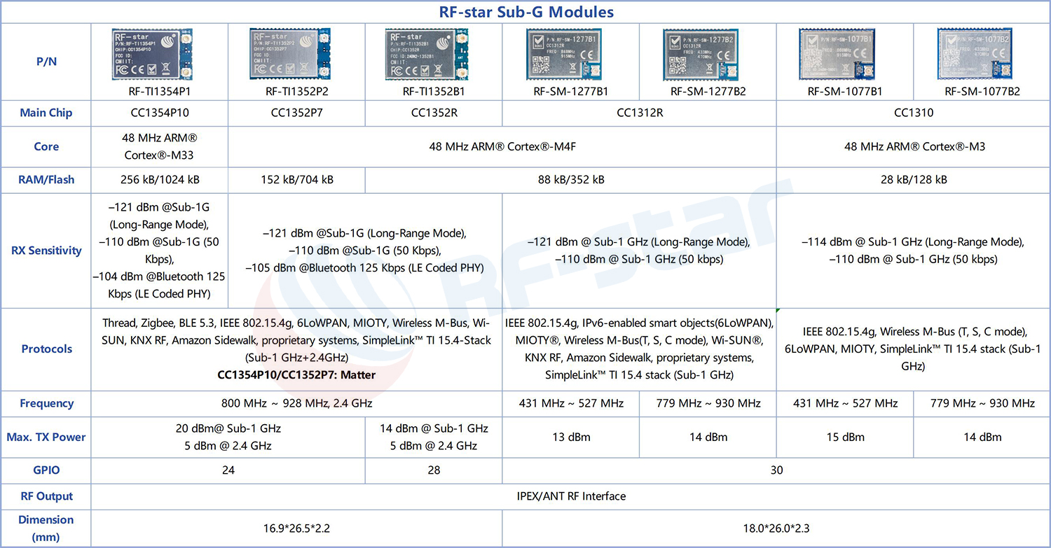
Wi-SUN (Wireless Smart Ubiquitous Network) This is an open standard protocol based on IEEE 802.15.4g standards, renowned for its powerful mesh network self-forming and self-healing capabilities and high scalability. It is very suitable for IoT applications requiring large scale, high reliability, and frequent communication between devices, such as Advanced Metering Infrastructure (AMI) and smart power distribution.
Representative Chips: TI's CC1312R, CC1352R, CC1352P, CC1352P7, CC1354P10 and other series chips, featuring +20 dBm transmit power, are an ideal hardware foundation for building Wi-SUN networks.
Other Standard Protocols Including Sigfox (Ultra-Narrowband technology), wireless M-Bus (European standard for smart metering), Z-Wave (smart home protocol), etc., each playing an important role in specific application fields.
Core Characteristics of Sub-G Modules
Ultra-Long Transmission Distance: Under the same transmit power, its communication distance far exceeds that of 2.4 GHz technologies, easily covering ranges of several kilometers.
Powerful Penetration and Diffraction Capability: Low-frequency signals can effectively bypass or penetrate obstacles like buildings and vegetation, performing stably in complex environments.
Ultra-Low Power Consumption: Many protocols are optimized for battery power, combined with deep sleep modes, enabling device battery life to last for years or even over a decade.
Strong Anti-Interference Capability: The Sub-G band is far from crowded bands like Wi-Fi and Bluetooth, with low environmental noise, making communication links very reliable.
Large Network Capacity: Based on various network architectures like Star topology, a single gateway can connect to tens of thousands or even hundreds of thousands of end nodes, facilitating large-scale deployment.
Excellent Interoperability (Specifically for standard protocols like Wi-SUN): Adhering to globally unified open standards, devices from different manufacturers can seamlessly access the same network, breaking down ecosystem barriers.
Typical Application Scenarios
Smart Cities and Utilities: Including remote reading for smart water/electricity/gas meters, smart street light control, smart parking, and urban environmental monitoring, representing the most classic application area for Sub-G modules.
Smart Agriculture and Livestock Farming: Enabling field soil moisture monitoring, meteorological data collection, smart irrigation control, and livestock location tracking.
Industrial IoT (IIoT): Used in vast factory areas or mines for equipment condition monitoring, asset tracking, and pipeline safety monitoring.
Smart Home and Security: Providing whole-house stable coverage for devices like smart door locks, door/window sensors, and smoke detectors, with strong signal penetration. The Z-Wave protocol is widely used in overseas smart homes.
RF-star Sub-G Module Solutions
RF-star Technology provides a series of mature and stable Sub-G modules. Their advantages in hardware design and integration greatly help customers simplify the product development process.
Rich Package Designs RF-star modules adopt standardized stamp-hole SMD packages with diverse sizes, making them very suitable for embedding into various structures. This integrated SMD package facilitates large-scale production using automated pick-and-place machines, effectively improving production efficiency and ensuring product consistency.
Flexible Antenna Options To accommodate different product design needs, RF-Star's Sub-G modules offer various antenna connection methods. For devices requiring built-in antennas, the PCB antenna on the module is convenient and cost-effective. For applications requiring optimal RF performance, the module is equipped with a standard generation IPEX interface, allowing easy connection to external rod antennas or flexible antennas, providing engineers with maximum design flexibility.
Plug-and-Play Reliability Choosing RF-Star Sub-G modules means developers do not need to invest high costs and effort into complex RF circuit design, and some modules also feature proprietary transparent transmission protocols. These critical and time-consuming steps have been completed on the module side, ensuring that end products can be brought to market quickly with excellent communication stability and reliability.
Rich Interface Support RF-Star's Sub-G modules provide comprehensive hardware interface resources for easy system integration, including but not limited to UART, SPI, I2C, and other standard interfaces. The abundant interface resources meet the connection needs of most IoT nodes. Multi-Protocol Compatible Platform Some of RF-Star's Sub-G modules support dual-mode concurrent operation (2.4 GHz + Sub-G), and can also support various communication protocols such as Wi-SUN and proprietary protocols. The same hardware platform can adapt to different market and application requirements, also reserving ample space for future product upgrades and feature expansion.
Summary and Outlook
In the current era of increasingly diversified IoT connectivity needs, Sub-G modules have become an indispensable part of wide-area IoT applications due to their comprehensive advantages in range, power consumption, penetration capability, and cost. The diverse, high-performance module solutions provided by RF-Star continue to empower developers, significantly lower the barrier to R&D, and drive the boundaries of the "Internet of Everything" to expand wider and deeper.
LEDs turn more power into light, not heat, so you get more brightness with less waste.
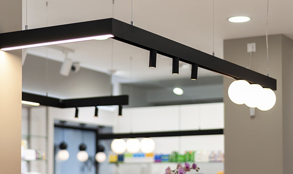
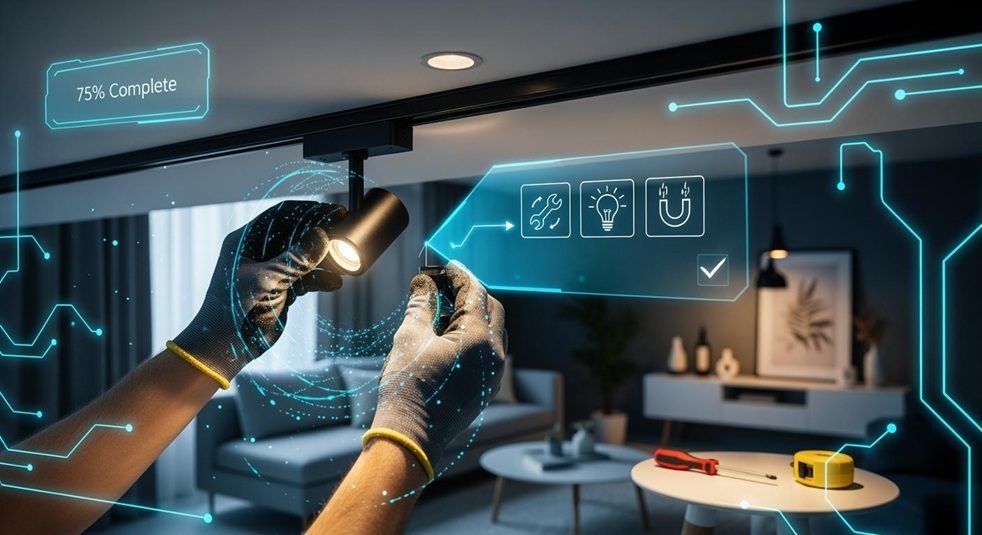
Proper installation makes a huge difference. When you start installing track lighting, you control both style and function. You’ve got this!
Key Takeaways
LED track lighting can help you save a lot of money. You can save about 75% to 90% on your energy bills. This makes it a good choice for your home. - You can change and control track lighting to fit your style. Smart technology lets you make the lights look special. You can also change the lights to fit what you need. - It is important to install and set up the lights the right way. This helps you get the best light in every room. - Clean your fixtures often to keep them shining bright. Taking care of them will help them last longer. - You can mix different fixture styles to make your lights work better. Using smart controls can also make your lights look nicer and work well.
Choosing LED Track Lighting Fixtures
Modern Design Trends
You want your space to look fresh and stylish, right? Modern trends in track lighting focus on flexibility and smart features. Take a look at this table to see what’s popular now:
Trend
Description
Customization
Modular systems let you mix and match parts for a unique look and easy changes.
Energy Efficiency
Sustainable materials and tech help you save energy and boost performance.
Smart Technology Integration
Intelligent lighting adjusts to your schedule or room use, making life easier.
If you love gadgets, smart controls in your track lighting system can change the mood with just a tap. Customization lets you swap out fixtures or move them around, so your room always feels new.
Fixture Types and Finishes
Choosing the right fixtures makes a big difference. You’ll find bold, artsy designs and sculptural shapes that stand out. Many people pick wall-mounted fixtures or floating styles for a sleek look. Stainless steel and chrome finishes add a modern touch, especially in kitchen track lighting. Unique forms can turn your lighting into a statement piece.
Tip: Big, eye-catching fixtures work well in open spaces. Smaller rooms look better with simple, streamlined designs.
Room Size and Lighting Needs
Room size matters when you plan your track lighting installation. Mount track lights at a height of 7 to 8 feet in most homes. Space fixtures 4 to 6 feet apart for even light. In narrow rooms, a straight line works best. For bigger areas, cluster fixtures to highlight special spots.
Here’s a quick guide for recommended brightness:
Room Type
Recommended Lumens Range
Key Purpose
Living Room
1,500–3,000
Relaxing, entertaining
Kitchen
5,000–10,000
Cooking, food prep
Home Office
3,000–6,000
Working, reading
Bedroom
1,000–2,000
Sleeping, dressing
Bathroom
2,000–4,000
Grooming, showers
You keep your space safe and comfortable by following these tips. When you focus on choosing the right fixtures and layout, your led track lighting fixtures will shine in any room.
Track Lighting Installation
Setting up track lighting is not too hard. If you have the right tools and a plan, you can do it. Safety is important, so follow some tips. Let’s look at each step together.
Tools and Materials
Get your tools ready before you start. The right tools make the job easier and faster. Here is a list to help you:
Drill and drill bits
Screwdriver (flathead and Phillips)
Wire stripper
Measuring tape
Pencil or marker
Ladder
Fish tape (for running wires)
Safety goggles and gloves
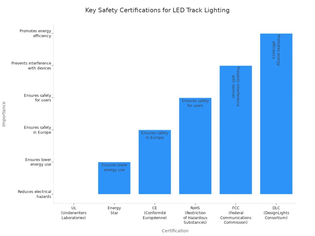
Tip: Always check if your tools and lighting have safety certifications. Certified tools help keep you safe from electrical problems. They also make sure your work meets the rules.
Here is a table that shows some important certifications:
Certification
Description
Importance
UL (Underwriters Laboratories)
Recognized safety certification for lighting products in the U.S. and Canada.
Reduces electrical hazards in installations.
Energy Star
U.S. government-backed certification for energy efficiency.
Ensures lower energy use and higher quality.
CE (Conformité Européenne)
Indicates compliance with EU safety and environmental standards.
Ensures safety and environmental protection in Europe.
RoHS (Restriction of Hazardous Substances)
Limits hazardous materials in electronic products.
Ensures safety for users and the environment.
FCC (Federal Communications Commission)
Ensures compliance with electromagnetic interference limits.
Prevents interference with other electronic devices.
DLC (DesignLights Consortium)
Focuses on high-efficiency commercial lighting products.
Promotes energy efficiency and potential utility rebates.
Planning Layout
A good plan helps your lights work well. Look at your room and think about what you want to light up. Here are some tips:
Assess Your Space: Check your room’s size and shape. See where you need more light.
Define Your Lighting Goals: Decide if you want to show off art, light a desk, or make the room feel cozy.
Choose the Right Fixtures: Use spotlights for small areas. Use floodlights for big spaces. Pendants add style.
Color Temperature and Bulb Selection: Warm white bulbs feel soft. Cool white bulbs are good for work.
Installation Tips: Put the track near things you want to highlight. Keep it at a safe height.
Think about how far the tracks should be from the wall. Here is what works best:
Place tracks 20 to 40 inches from the wall if your ceiling is normal height.
This makes it easy to point the lights where you want.
You will also stop glare on pictures or art.
Note: Measure two times before you drill holes. If you need to cut the track, use a hacksaw. Smooth the edges with a file.
Mounting and Wiring
Now you can put up your track lighting system. Follow these steps to stay safe and do a good job:
Remove Existing Fixtures: Take down old lights. Watch how the wires are connected.
Run the Electrical Cable: Drill a hole if you need to. Use fish tape to pull the cable from the switch box to the ceiling.
Mount the Tracks: Put the cable in the track. Mark where the screws go, drill holes, and attach the track to the ceiling.
Wire the Track System: Connect the ceiling wires to the track. Match the colors and make sure the wires are tight.
Attach and Aim Track Heads: Snap the lights into the track. Test the lights and point them where you want.
Safety Precautions: Always turn off the power at the breaker before you start. Wear safety goggles and gloves. Make sure you can reach the driver for future checks.
When you wire, follow the National Electrical Code (NEC). This code tells you how to wire, ground, and protect your system. Article 410 is about track lighting systems. Always ground metal parts to stop shocks. Use the right protection to keep your system safe.
Now you know all the steps for a safe and nice installation. With a good plan and the right tools, your led track lighting fixtures will make your room look great.
Customizing LED Track Lighting Fixtures
Adjusting Direction and Beam Angle
You have a lot of control with led track lighting fixtures. You can point the lights exactly where you want. This is great if you like to change your room or move your furniture. Adjusting the direction and beam angle lets you highlight a painting, a reading nook, or even your kitchen counter. When you focus the beam on a piece of art, you create a dramatic effect. The light seems to come from the artwork itself, making it pop. This is called artwork spotlight lighting, and it works well in living rooms, hallways, or galleries.
A smaller beam angle gives you a strong, focused light. Use this to show off a special feature or make a bold statement. A wider beam angle spreads the light out. This makes the room feel softer and more relaxed. For example, a 25-degree beam angle is perfect for highlighting a sculpture, while a 120-degree angle works better for general lighting in a big space. Always check that your angle-adjusting accessories fit your fixtures and match your room’s style. You can change the mood of a room just by turning or tilting the lights.
Tip: Try different angles and see how the light changes. You might find a new favorite look!
Mixing Fixture Styles
You do not have to stick with just one style on your track lighting system. Mixing different fixture styles gives you more options and makes your space interesting. You can use spotlights for tasks, pendants for style, and wall sconces for a cozy feel. This kind of customization lets you layer your lighting. You get both bright light for working and a soft glow for relaxing.
Interior designers often suggest these combinations for modern spaces:
Pendants, wall sconces, and accent lighting
Bright colors that match your room’s color scheme
Accent lighting to highlight cool features or artwork
Unique wall sconces and warm lights for a cozy mood
When you mix styles, you can create a look that is all your own. You can even use kitchen track lighting with bold pendants and sleek spotlights to make your kitchen stand out.
Smart Controls and Dimmers
Smart controls make your lighting easy to use and fun to play with. You can control your lights with a remote, your phone, or even your voice. Many led fixtures now come with smart features. You can dim the lights, change the color temperature, or set a schedule. This helps you save energy and makes your home more comfortable.
Here is a quick look at some smart features you might find:
Feature
Description
Light beam
Zoomable from 15° to 38°
Control system
Smart remote-controlled system
Dimmability
Dimmable LED Track Light
Color Temperature (CCT)
Changeable from 2700K to 6000K
Lighting head
360° rotatable
Vertical adjustment
90° adjustable
Smart controls let you set the mood for any time of day. You can dim the lights for movie night or brighten them for homework. Dimmers also help you use less electricity, which means lower bills. You can even track your energy use and make better choices. Setting up scenes or schedules adds convenience and makes your lighting work for you.
Note: Smart dimmers and controls are easy to add during installation. Always follow safety tips and check that your system is compatible.
Color Temperature and Brightness
Color temperature and brightness change how a room feels. Warm light (2700K to 3000K) makes a space feel cozy and inviting. Cool light (above 4000K) helps you stay alert and focused. You can pick the right color temperature for each room:
Space
Recommended Color Temperature (K)
Living Room
2700K - 3000K
Kitchen
2700K - 4000K
Office
3000K - 5000K
You can also adjust the brightness to match what you are doing. Use bright, ambient lighting for cleaning or working. Switch to softer light for relaxing or watching TV. Layering your light—using ambient, task, and accent lighting—gives you the most control. For example:
Ambient lighting sets the mood and fills the room with light.
Task lighting helps you see better for cooking or reading.
Accent lighting draws attention to special features or decorations.
With the right setup, your track lighting can do it all. You get style, comfort, and flexibility in every room.
Maintenance and Troubleshooting
Cleaning and Care
Keeping your LED track lighting clean helps it shine bright and last longer. Dust and dirt can block the light and make your room look dull. You should clean your fixtures regularly, just like you would with any other lights. Dirty lenses or covers can lower the amount of light you get, so a quick cleaning makes a big difference.
Here’s a simple way to keep your lights in top shape:
Gather a microfiber towel. This soft cloth will not scratch your fixtures.
Turn off the power and let the lights cool down before you start.
Use a sturdy ladder. Ask someone to help if you need extra support.
Mix a mild cleaner with warm water. Only use this on parts you can remove. Keep water away from wires and electrical parts.
After cleaning, check that all screws and parts are tight and secure.
Tip: Make cleaning your track lighting a regular task. You will keep your space bright and safe!
Common Issues
Sometimes, you might notice your lights flicker, look dim, or stop working. Most problems have easy fixes. Here are some common issues and what you can do:
Clean the track and fixtures often. Dust can cause connection problems.
Do not overload the track. Stay within the wattage limit to avoid trouble.
Make sure there is space around the lights. Good airflow stops them from getting too hot.
Replace dim bulbs right away. This keeps the driver from working too hard.
If a light will not turn on, check the power source and clean the contacts.
Flickering lights? Make sure your bulbs work with your dimmer switch. Some LEDs need special dimmers.
If you hear buzzing or see dim light, you might need a new driver or bulb.
If you cannot fix the problem, call a professional for help.
Note: Always use bulbs and dimmers that match your system. This helps your track lighting work its best.
You can transform any room with LED track lighting. Here’s a quick recap of the main steps:
Plan your layout and measure your space.
Install the track securely on the ceiling.
Connect the wiring as the instructions show.
Add and adjust your lights for the perfect look.
Modern LED track lighting gives you style, energy savings, and smart control. You can customize your setup to fit your needs. Check out some top reasons to start your project:
Motivation
Description
Versatility
Adjust and direct light where you want it.
Aesthetically Pleasing
Modern design boosts your room’s style.
Energy Efficiency
Save money with LED bulbs.
Adaptable
Change your lighting as your space changes.
Task Lighting
Focus light for work or hobbies.
Ready to brighten your home? Start your LED track lighting project today and enjoy a space that feels both modern and personal! ✨
Shows the real colors of things, making spaces look lively and nice.
Ideal for Commercial Spaces
Great for stores and galleries where color is important.
Enhances Product Appeal
Makes products stand out and look their best.
Customization & Flexibility
You can change Magnetic Track light systems in many ways. Pick from different track sizes, colors, and lengths. Choose black, white, bronze, champagne, or gold to match your style. Tracks come in 1 or 2 meters, and you can cut them shorter. Put them on the surface, inside the ceiling, or hang them down. You can add, move, or take away light modules easily. Change the beam angle, color temperature, or dimming type to fit your needs. This makes it easy to update your lights when your space changes.
Move fixtures without extra work.
Change lighting for new furniture or layouts.
Good for homes, offices, and stores.
Smart Control Options
Smart control options make Magnetic Track light systems even better. You can use your phone, a remote, or your voice to control the lights. Many systems use Bluetooth or Wi-Fi for easy setup. Set scenes for reading, relaxing, or working. Smart controls help you save energy and money. You can set lights to turn on or off at certain times. Some systems work with your smart home devices for more ease.
Feature
Description
Control Methods
Use your phone, remote, or voice to change the lights.
Connectivity
Connect with Bluetooth or Wi-Fi for easy setup.
Scene Setting
Make custom lighting scenes for different activities.
Magnetic Track light trends in 2025 focus on style, flexibility, and smart features. You can make a space that looks good and works for you.
Why Choose Magnetic Track Light
Seamless Aesthetics
You want your room to look neat and new. Magnetic Track light systems help you do this. These lights fit into your ceiling or wall. You see the light, not big fixtures. The design matches many styles, like Scandinavian or industrial. The lights do not stand out. Your space looks planned and part of your home.
Magnetic track lights keep your room tidy.
The fixtures do not take attention from your art or furniture.
You can link tracks from ceilings to walls for a smooth look.
Tip: Pick magnetic track lights if you want your room to feel open and neat.
The table below shows why people like magnetic track lighting more than old lights:
Advantage
Description
Easy Installation
You can attach them fast with magnets.
Flexible Adjustability
You can move fixtures along the track easily.
Sleek Aesthetics
They make your room look modern and clean.
Versatile Applications
Good for rooms that need changing lights.
Convenient Maintenance
It is easy to change bulbs or adjust them.
Versatile Applications
You can use modern magnetic track lights in many places. They work well in homes, offices, and stores. You can change the lights when you need to. This makes them smart for spaces that change over time.
Here are some places where you might see magnetic track lights:
Type of Space
Description
High-end residential homes
These homes often use modern lighting.
Contemporary offices
Offices use flexible lights for different jobs.
Design studios
Studios need lights they can change for work.
Upscale commercial interiors
These places want modern looks and good use.
Luxury apartments
These homes want hidden hardware and modern lights.
Design showrooms
Showrooms need flexible and custom layouts.
You can move or add fixtures without tools. This lets you make new lighting for different things you do. You can also change your lights when you move your furniture. Magnetic Track light systems let you set up your space how you want.
Practical Benefits
Safety Features
You want your lighting to be safe for everyone at home or work. Magnetic track lighting systems help you avoid many common risks. These systems do not need tools for installation, so you lower the chance of electrical fires or other hazards. You can adjust the lights without touching wires or using sharp tools. The fixtures stay locked in place with strong magnets. This means you do not have to worry about lights falling or moving by accident, even in busy spaces.
No tools needed for setup, so you avoid electrical risks.
Fixtures stay secure, which helps prevent accidents.
You can safely adjust lights as often as you need.
Tip: Magnetic track lights are a smart choice for families with kids or for busy offices.
Easy Installation
You can install magnetic track lights much faster than traditional lighting. The process is simple and does not require special skills. You just snap the tracks and fixtures into place. If you want to move a light, you can do it without any tools. Traditional lighting often needs extra effort and time to adjust fixtures after installation. Magnetic track lights let you change your setup quickly. This makes them perfect if you like to update your space often.
Feature
Magnetic Track Lights
Traditional Lights
Tool-Free Adjustment
Yes
No
Installation Time
Short
Long
User-Friendly
Yes
No
Energy Efficiency
You can save a lot of energy with magnetic track lighting. Most systems use LED bulbs, which use much less power than old-style lights. You might save up to 90% on your energy bills compared to traditional lighting. LEDs also last longer, so you do not have to replace bulbs as often. This helps you save money and helps the environment at the same time.
LED bulbs use less electricity.
Lower energy bills for your home or business.
Fewer bulb changes mean less waste.
Note: Choosing energy-efficient lighting is good for your wallet and the planet.
Impact on Interiors
Personalized Spaces
You can shape your home to match your style with Magnetic Track light systems. These lights do more than brighten a room. You can use them to highlight art, show off special furniture, or draw attention to unique walls. Many people now use track lighting as a design feature, not just a tool. You can move the lights or change their direction whenever you want. This lets you try new looks without much effort.
You might want a cozy reading corner one day and a bright workspace the next. Magnetic Track light systems let you make these changes quickly. You do not need to call an expert. You can swap out fixtures or adjust the layout as your taste changes. This flexibility helps you create a space that feels truly yours.
Tip: Try different lighting setups to see how they change the mood in your room.
Sustainable Design
You help the planet when you choose modern lighting. Many new systems use LED technology. LEDs use less energy and last longer than old bulbs. You save money and reduce waste at the same time. Magnetic Track light systems also use smart controls. You can set timers or use sensors to turn off lights when you do not need them.
Here is how these systems support green living:
Feature
Description
LED Technology
Uses less power and lasts longer than regular bulbs.
Flexibility
Lets you light only the areas you need, saving energy.
Reduced Replacement
Easy to update, so you do not throw away old fixtures as often.
Smart Integration
Works with smart home systems for better energy use.
Recyclable Materials
Some tracks and fixtures use materials you can recycle.
You make your home more eco-friendly by picking lighting that uses less energy and creates less waste. Smart lighting also helps you use only what you need, which is good for both your wallet and the environment.
Selecting Magnetic Track Light
Key Considerations
When you choose a magnetic track lighting system, you want to make sure it fits your space and needs. Start by thinking about the track length and layout. Measure your room and decide how much of the area you want to light. A longer track can cover more space, while a shorter one works well for small rooms.
Next, look at the types of fixtures you need. Some fixtures give general light, while others focus on certain spots. You can pick spotlights for art, linear lights for even coverage, or pendant lights for a stylish touch. Each type helps you create the right mood in your room.
Control options matter, too. Many systems let you dim the lights or change the color temperature. Some even connect to smart home devices. These features make it easy to set the perfect scene for reading, relaxing, or working.
Track length and layout: Match the track to your room size and lighting needs.
Fixture types: Choose spotlights, linear, or pendant lights for different effects.
Control options: Look for dimming, color changes, and smart home features.
Tip: Think about how you use each room before picking your lighting setup.
Integration Tips
You can get the best results by following a few simple tips when you install magnetic track lights. First, pick the right track type. Most people use 48 V tracks because they work well and are safe.
Pay attention to the beam angle. Movable lights let you point the light where you want, but you should avoid glare or unwanted reflections. Choose a color temperature that matches your style. Warm light feels cozy, while cool light feels bright and fresh.
Keep about 5 inches between each light for even coverage. If your room has high ceilings, make sure the lights are strong enough to reach the floor. Reflector panels can help spread the light and make your space look brighter.
Use 48 V tracks for most projects.
Adjust beam angles to avoid glare.
Pick warm or cool color temperatures for the right mood.
Space lights about 5 inches apart.
Check room height for proper light coverage.
Add reflector panels for better light spread.
Choose energy-saving bulbs to lower costs.
Decide if you want recessed, surface, or hanging tracks.
Note: Careful planning helps your magnetic track lights look great and work well in any room.
Magnetic track lighting lets you change your room’s look and use. You get a modern style, can move lights, and save energy. Many people pick these lights because they are easy to adjust. They also look cool and new.
Put tracks to shine on art or make a cozy spot.
Use curvy tracks in halls or over beds for something special.
Some workers might need to learn more to install them right.
Pick magnetic track lighting if you want a space that feels new and easy to change. Try new things and let your lights change as you do.
You can put in a dimmable magnetic led track light by following some easy steps and using the right tools. This new light uses magnets to attach lights to a track. You can move and change the lights easily. Before you begin, plan your setup and think about safety.
Tip: Always look for dangers like bad wiring or too much power in circuits. Use the right gear and work carefully to stay safe.
Safety Incident
Description
Electrical Shocks
You can get shocked by live wires. Use the right tools and follow safety rules.
Falling from a Ladder
Working high up can make you fall. Use safety gear and be careful.
Fire Hazards
Sparks and fires can happen. Use safe fixtures and make good connections.
Magnetic Track Light Basics
What Is a Magnetic Track Light
You might wonder what makes a modern recessed magnetic track light different from other lights. This system uses a special track with magnets inside. You can attach light fixtures to the track and move them around without tools. The track rail is usually made from aluminum and has copper strips for power. The lamp body has a magnetic adapter, so you can snap it into place and slide it wherever you want. The power supply changes regular electricity into low voltage, which makes the system safer.
Here are the main parts you’ll find in a Magnetic Track Light system:
Magnetic Track Rails: These come in different sizes and styles for your space.
Power Supply: This converts your home’s electricity to a safe level for the lights.
Connect Track Rail Accessories: You use these to join tracks and create your layout.
Magnetic LED Lamps: Pick from many types to get the look and brightness you want.
Tip: You can install these tracks on the ceiling or wall. You can even hang them as pendants for a cool effect.
Key Benefits
When you choose a Magnetic Track Light, you get more than just good lighting. You get flexibility, style, and savings. You can move the lights to highlight artwork, brighten a reading nook, or change the mood in your room. You don’t need tools to adjust the lights, so you can change your setup anytime.
Here’s a quick look at why people love Magnetic Track Lights:
Benefit
Description
Flexibility
Move lights along the track to fit your needs.
Energy Efficiency
Use less energy and save up to 30% compared to old halogen lights.
Modern Aesthetics
Enjoy a sleek, clean look with hidden wires and a minimalist design.
Easy Installation
Snap lights into place without complicated wiring or tools.
Versatility
Use in homes, offices, or shops for different lighting effects.
Smart Integration
Connect with smart home systems for remote control and scheduling.
You also get a safer system because Magnetic Track Lights use low voltage. This means less risk of shocks. The design fits almost any style, so your space looks modern and tidy. You can add or remove lights as your needs change, and you won’t need an electrician every time.
Tools and Materials
Before you begin, gather all your tools and materials. This helps you work faster and make fewer mistakes. Let’s see what you need for a safe and simple job.
Essential Tools
You do not need special tools, just some basics. These tools will help you finish the job easily. Here is a list to help you get ready:
Screwdriver (for turning screws)
Electric drill and drill bits (for making holes)
Measuring tape or ruler (to measure where things go)
Pencil (to mark spots)
Level (to keep the track straight)
Wire stripper (to remove wire covers)
Electrical tester (to check if wires have power)
Screws and anchors (to hold the track in place)
Wire nuts (to connect wires safely)
Magnetic track light kit (with tracks, connectors, and lights)
Tip: Always check your measurements before you drill. Even a small mistake can change how your lights look.
Required Materials
You want your Magnetic Track Light to last and look nice. Good materials help your system work better. Here is a table with the most used materials:
Material
Description
FR4 circuit boards
These do not rust and carry electricity well.
6063 aviation-grade aluminum
This aluminum is strong and keeps your track safe.
You also need power cables, insulation tape, and thin magnetic lamps for your track.
Safety Gear
Safety is very important when working with electricity. Wear the right gear to protect yourself:
Insulated gloves (to stop shocks)
Flame-resistant clothing (for more safety)
Hard hat (if you work above your head)
Safety glasses (to protect your eyes)
Protective footwear (to keep your feet safe)
Note: Never forget your safety gear. Even a fast job can be dangerous if you are not careful.
Planning the Installation
Confirm Design Pattern
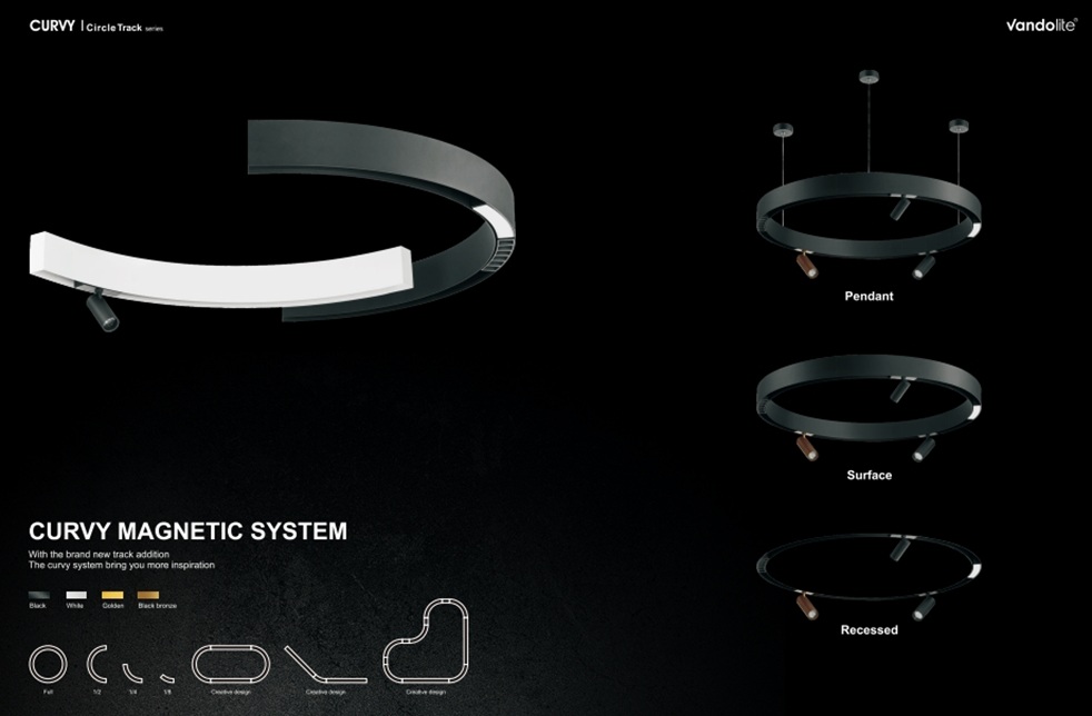
You want your Magnetic Track Light to look great and work well. Start by picking a design pattern that fits your room. Think about how you use the space and where you need the most light. Some people like a straight line of lights for a clean look. Others choose shapes like L-shape or U-shape to light up corners or large areas. You can even try a snake shape for a fun, wavy effect.
Here’s a quick table to help you decide:
Design Pattern
Description
Linear
A straight line of lights along the track.
L-shape
Good for corners and corridors.
Oval
Soft, rounded lighting effect.
Round
Creates a focal point in the room.
Square
Fits modern spaces and offices.
Snake shaped
Wavy design for a dynamic look.
You can also use a grid or modular pattern for bigger rooms. If you want to highlight a sofa or a dining table, try a U-shape or I shape. Take a moment to sketch your plan on paper. This helps you see how the lights will look before you start.
Choose Track Rail and Lights
Now, pick the right track rail and lights for your setup. Not all rails work with every light fixture. You need to match the track type with the right heads. For example, H tracks only fit H-style heads. J tracks need J-style heads. L tracks go with L-style heads. Some adapters let you mix and match, but it’s better to stick with the same style for best results.
Track Type
Compatibility with Fixtures
Notes
H
H-style heads
Only compatible with H-style tracks
J
J-style heads
Only compatible with J-style tracks
L
L-style heads
Only compatible with L-style tracks
-
Mixed compatibility
Adapters may work, but not ideal
Pick lights that match your style and brightness needs. You can choose spotlights for art or wide lights for general use. Make sure your lights and rails work together before you buy them.
Mark and Prepare Area
Get ready to install by marking your area. Use a measuring tape to find the right spots for your track. Draw lines with a pencil where you want the rails to go. Check that your lines are straight with a level. If you want a shape like L or U, measure each side carefully. Double-check your marks before you drill any holes.
Tip: Take your time with measuring and marking. A small mistake can make your lights look uneven or out of place.
Clear the area of furniture and dust. Make sure you have enough space to work safely. If you plan well, your Magnetic Track Light will look neat and work perfectly.
Installing the Magnetic Track Light
Power Off and Safety
Before you start, turn off the power at the breaker. You want to make sure no electricity flows to the area where you will work. Use an electrical tester to double-check that the wires are not live. Put on your insulated gloves and safety glasses. If you work above your head, wear a hard hat. Safety comes first, so never skip these steps.
Tip: Always check the power twice. If you feel unsure, ask someone to help you confirm.
Attach Power Adapter
Find the spot where you want to connect the power adapter. Most Magnetic Track Light systems use a low-voltage adapter, like 12V or 24V. Some LED spotlights for living room connect straight to 110V or 220V, but many need a transformer. Look at your product’s label to see what you need.
Here’s a quick table to help you match your power supply:
Voltage Type
Voltage Specification
Current Requirement
Example Product
Low-Voltage
12V/24V
Needs separate transformer
Combo Track Lights (12V) for a 10㎡ bedroom, 60W transformer
High-Voltage
110V/220V
No transformer needed
Uranus Track Light (220V) for a 30㎡ retail store
Connect the adapter to the main power wires. Use wire nuts to keep the wires safe and tight. Wrap insulation tape around the connections. Make sure the adapter sits close to the track rail for easy wiring.
Mount Track Rail
Now, you need to mount the track rail to the ceiling. The way you do this depends on your ceiling type. Here’s a table to help you pick the best method:
Installation Method
Description
Suitable Ceiling Types
Embedded Magnetic Rail
Fits inside the ceiling for a flush look
Drywall, plaster ceilings
Surface Mounted Magnetic Rail
Attaches right on top of the ceiling
Concrete, wood ceilings
Hoisted Magnetic Rail
Hangs down for adjustable height
High ceilings, industrial spaces
Most people use surface mounting because it’s simple and works for many homes. If you want a modern look, try recessed mounting. For tall rooms, hoisted rails look great.
Follow these steps to mount your track:
Measure and mark the spot for the rail using a tape and pencil.
Use a level to make sure your marks are straight.
Drill pilot holes at each mark.
Hold the rail in place and screw it into the ceiling. Make sure it sits flat and does not wobble.
Check that the rail feels secure before you move on.
Note: If your ceiling is soft, use anchors to keep the screws tight.
Connect Tracks with Adapter
If you use more than one track rail, you need to connect them with adapters. Push the copper rails forward so they touch the adapter well. Sometimes, tracks slide too far down and lose contact. If you see this, push them back up and try again. Make sure each phase of the rail connects with the end feed. If the lights do not work, re-seat the connection.
Common mistakes to avoid:
Tracks sliding too far down, causing poor contact.
Not connecting the rail phase with the end feed.
Forgetting to push copper rails forward.
Take your time with this step. Good connections mean your lights will work every time.
Connect Power Supply
After you connect the tracks, hook up the power supply. If you use a low-voltage system, connect the transformer to the adapter. For high-voltage systems, connect the wires straight to the rail. Use wire nuts and insulation tape for safety. Double-check all connections before you turn the power back on.
Alert: Never touch bare wires. Always use tools with insulated handles.
Install Magnetic Lights
You’re almost done! Now, snap the magnetic lights onto the track. Hold each light fixture close to the rail. The magnets will grab the track and hold the light in place. Slide the lights to the spots you want. Make sure each light sits straight and feels secure.
Follow these steps for perfect alignment:
Gather your lights and check that they match your track.
Place each light against the rail. Let the magnets pull it into place.
Slide the lights to your chosen spots.
Turn the power on and test each light.
If a light does not work, check the connection and try again.
Tip: Test the lights before you finish cleaning up. If you see flickering or no light, check the adapter and rail connections.
Your Magnetic Track Light system is now ready. You can move the lights anytime to change your room’s look. Enjoy your new lighting!
Testing and Troubleshooting
Power On and Test
You finished installing your magnetic track lights. Now, it’s time to see if everything works. First, stand back and double-check that all wires are covered and the track feels secure. Put on your safety gear one more time. Go to your breaker box and turn the power back on.
Walk back to your lights. Flip the wall switch or use your remote if you have one. Watch for each light to turn on. If you see all the lights glow, you did a great job! If some lights stay off or flicker, don’t worry. You can fix most problems with a few quick checks.
Here’s a simple checklist to help you test your lights:
Look for any lights that do not turn on.
Check for flickering or dim lights.
Listen for buzzing or crackling sounds.
Make sure all lights sit straight on the track.
Tip: If you see a problem, turn off the power before you touch anything.
Fix Common Issues
Sometimes, things don’t go as planned. You might run into a few common problems. Most of these have easy fixes. Take a look at the table below to see what you might face and how to solve it:
Issue
Solution
Compatibility issues
Make sure all your parts match. Use the same brand or check the specs.
Circuit overloading
Add up the wattage of your lights. Stay under the limit for your circuit.
Use of low-quality materials
Pick strong, high-quality tracks. Cheap ones can bend or break.
Improper installation
Check that your rails are straight and tight. Reinstall if needed.
Lack of maintenance
Look at your tracks often. Tighten loose parts and clean dust away.
If you find a light that won’t turn on, try moving it to another spot on the track. Sometimes, the magnets don’t make good contact. If you hear buzzing, check your wiring and connections. Always use good materials and follow the steps. You’ll have bright, safe lights that last a long time.
Note: Regular checks help you catch small problems before they get big. Keep your lights clean and tight for the best results.
Maintenance Tips
Cleaning
You want your magnetic track lights to stay bright and clean. Cleaning them is simple if you follow these steps. Always turn off the power before you start. This keeps you safe. Take off the light fixtures gently. Use a big soft brush to dust off dirt. Get a damp washcloth or a cleaning wipe. Wipe the fixture in one direction only. Do not use too much water. Water can cause problems with electricity. Let everything dry all the way before you put the lights back.
Turn off the power first.
Take off the fixtures and sockets slowly.
Use a soft brush to dust off dirt.
Wipe with a damp cloth or cleaning wipe in one direction.
Do not soak the fixture.
Let it dry fully before turning the power back on.
Tip: Clean your lights often. This helps them look new and last longer.
Routine Checks
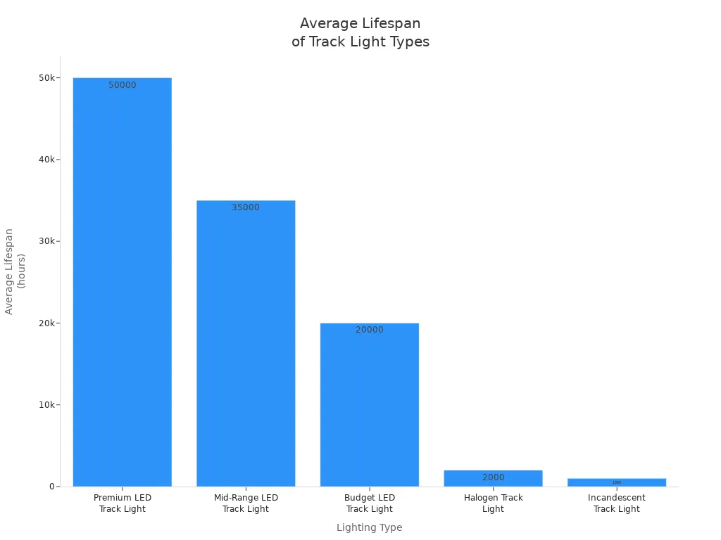
Check your magnetic track lights every few months. Look for loose parts, dust, or flickering bulbs. Tighten any screws that are loose. Make sure the magnets hold the lights tight. If you see damage, change the broken part right away. LED magnetic track lights last much longer than old bulbs. Look at this chart to see how long each type lasts:
Lighting Type
Average Lifespan (L70)
Hours Used/Day
Years of Use
Replacement Frequency (20-Year Period)
Premium LED Track Light
50,000 hours
6
22.8
0–1
Halogen Track Light
2,000 hours
6
0.9
22
Incandescent Track Light
1,000 hours
6
0.45
44
LED track lights can last over 25,000 hours. You will not need to change them often. This means less work for you!
Upgrading Fixtures
You may want to upgrade your magnetic track lights for better looks or features. New fixtures have cool things like smart controls and lights you can change. Some even stop flickering. Here are some new features you can get:
Feature
Description
Robust Construction
Strong aluminum helps keep lights cool.
Stable Magnetic Connection
Easy to move and stays in place.
Reliable Power Delivery
Gives steady low-voltage power.
Exceptional Color Rendering
Colors look bright and real.
Precise Beam Control
You can change the angle of the light.
Flicker-Free Operation
No flicker, so your eyes feel good.
Tunable White & Dimming
Change the color and brightness easily.
Smart Control Compatibility
Works with smart home systems.
Variety of Fixture Types
Choose from spotlights, linear lights, and more.
Thermal Management
Good cooling helps lights last longer.
Compliance & Safety
Meets safety rules from around the world.
Note: Upgrading your lights can make your room look new and save energy. You can change old lights for new ones in just a few minutes!
You did it! You installed your magnetic track lights and made your space shine. Remember these safety tips:
Wear gloves and safety glasses.
Keep flammable items away from the lights.
Check all wires and connections for tightness.
Inspect for loose fixtures or damaged parts.
Use the right voltage for your system.
Keep your lights clean and check them often. Want more style? Try adding glass-head lamps or smart-controlled lights. Here are some ideas:
Lighting Idea
Description
Glass-head track lamps
Add sparkle and personality to any room.
Bluetooth/Wi-Fi controlled lights
Change brightness and color with your phone.
Metal shades with vintage finishes
Give your space a bold, creative look.
Share your results with friends or try new lighting ideas to make your home even brighter!
Modern rooms benefit from magnetic track lights. These lights work well with soft colors and straight lines, creating a clean, contemporary look.
Industrial style interiors often feature black metallic lights. When you pair these with brick walls, you achieve a raw, urban vibe that fits the industrial design perfectly.
Magnetic led pendant lights offer versatility. You can use them as statement pieces in dining areas or living rooms, adding elegance and focus to your design.
For minimalist spaces, magnetic led pendant lights with simple shapes and neutral finishes blend seamlessly into the background, supporting a clutter-free design.
If you want to highlight artwork or architectural features, magnetic track lights provide targeted illumination and enhance your decor.
Tip: Always consider your room’s color palette and furniture style when selecting lighting. The right design choice can elevate your home and stay within your budget.
Adjustable & Positionable Features
You need flexibility in your lighting to adapt to changing needs. Magnetic led pendant lights and magnetic track lights offer several adjustable and positionable features that let you customize your lighting effects.
Feature
Description
Flexible Arm
Directs light exactly where you need it, improving task and accent lighting.
Magnetic Base
Lets you reposition lights easily, increasing versatility throughout your home.
Zoomable LED Flashlight
Adjusts beam modes for different lighting needs, from focused to ambient.
Universal Steel Mounting Plate
Attaches to various surfaces, allowing shared use across rooms or setups.
500 Lumens Brightness
Delivers strong, adjustable illumination for specific tasks or moods.
Quick Release Clip
Allows you to use the pendant independently for small tasks or accent lighting.
When you choose the best magnetic led pendant lights, you gain control over both the direction and intensity of your lighting. Adjustable features help you create the perfect atmosphere for any occasion. You can highlight a dining table, spotlight artwork, or simply brighten a reading nook. This flexibility ensures your design remains both functional and stylish.
Energy Efficiency & Features
When you select lighting for your home, you want to maximize efficiency and minimize waste. Magnetic LED circular lights stand out as some of the most energy-efficient lights available. In Europe, manufacturers rate LEDs on an A to G scale, with A representing the highest efficiency. Anything rated E or above meets the standard for energy efficiency. LEDs can reach up to 90% efficiency, while traditional incandescent bulbs often fall below 10%. This difference means you use less electricity for the same brightness, which helps you lower your utility bill
You may notice that the initial investment in LED magnetic lights is higher than older lighting options. However, the long-term savings quickly justify the cost. You benefit from lower electricity bills and fewer replacements because LEDs last much longer. For example, World Star Tech reported annual savings of $38,375 after switching to LED lighting. This case shows how energy-efficient lights can make a real impact on your budget over time.
Tip: Always check the energy rating label before you buy new lights. Choosing high-efficiency models ensures you get the best value for your home.
Dimmable & Smart Controls
You can further enhance your lighting experience by choosing dimmable and smart control features. Dimmable magnetic LED circular lights let you adjust brightness to match your mood or activity. This flexibility helps you create the perfect atmosphere, whether you want bright light for reading or a softer glow for relaxing.
Smart controls add another layer of convenience. Many modern LED lights work with smart home systems, allowing you to control them with your phone or voice commands. You can set schedules, automate lighting scenes, or adjust settings remotely. These features not only improve comfort but also help you save energy by ensuring lights are only on when needed.
Note: Dimmable and smart-enabled lights give you more control and help you use energy wisely. Look for these features when upgrading your home lighting.
Quality & Warranty
You want to invest in lighting that delivers consistent quality and reliability. Trusted brands earn their reputation by meeting strict industry standards and providing dependable products for your home. When you evaluate magnetic LED circular lights, look for manufacturers who have earned certifications from respected organizations. These certifications confirm that the lights meet international safety and performance standards.
Certification Body
Description
IEC
International Electrotechnical Commission, focuses on electronic products including LEDs.
CIE
International Commission on Illumination, dedicated to light and lighting standards.
ISO
International Organization for Standardization, sets global standards.
Zhaga
Consortium for standardizing LED luminaire interfaces.
UL
Underwriter Laboratories, provides safety testing and certification for LED products in the U.S.
CE
European conformity mark indicating compliance with safety standards in the EU.
Brands that display these certifications show a commitment to quality and safety. You should also check customer reviews and ratings to gauge real-world performance. Reliable brands often offer responsive support and clear documentation, which helps you feel confident about your purchase.
Tip: Choose brands with a proven track record and recognized certifications to ensure your lighting meets high standards for your home.
Warranty Terms
Warranty coverage protects your investment and ensures you receive lasting quality from your lights. Manufacturers who stand behind their products usually offer comprehensive warranties that cover both labor and materials. You should review the warranty terms before making a decision, as strong coverage reflects the company's confidence in their lighting.
One-Year Labor Warranty: Covers all labor and workmanship for installation or repair, so you avoid extra costs if errors occur.
Five-Year Product Warranty: Protects against manufacturing defects in LED fixtures and components, including replacements or repairs.
Financial Security: Warranties prevent unexpected expenses for repairs or replacements, helping you stay within your budget.
Guaranteed Quality: Shows the company's commitment to high-quality workmanship and reliable lighting.
Prolonged Lifespan: Encourages regular maintenance and prompt repairs, which extends the life of your lighting systems.
Enhanced Customer Confidence: Gives you peace of mind, allowing you to rely on your lights for years.
You should always read the warranty terms carefully and keep documentation for future reference. Strong warranties and reputable brands help you maintain quality lighting in your home and protect your budget over time.
When you choose amagnetic led circular light, you take several important steps. You compare magnetic track lights, magnetic led pendant lights, and other options to understand features, advantages, and drawbacks. This approach helps you match lighting to your home’s needs, color preferences, and budget. Take time to check compatibility and ensure the design fits your space. Avoid mistakes like ignoring ambient temperature, overlooking voltage, or neglecting environmental conditions. The table below shows how the right choice brings lasting benefits:
Benefit
Description
Energy Efficiency
Consumes less power, lowering bills and reducing emissions.
Durability
Lasts longer, reducing waste and replacements.
Aesthetic Versatility
Integrates into any design, improving both quality and function.
You create a comfortable home with quality lighting, magnetic track lights, and magnetic led pendant lights. Enjoy the improved design, reliable pendant performance, and lasting quality that magnetic led pendant lights bring to your daily life.