Scanning Electron Microscopy (SEM): Measures crystal size and morphology, and can be combined with energy-dispersive X-ray spectroscopy (EDS) for elemental composition and distribution.
Diffuse Reflectance Infrared Fourier Transform Spectroscopy (DRIFTS): Confirms the presence or absence of IR-active functional groups in the framework.
Below is a brief overview of sample preparation and key data analysis points for each characterization method.
1. Powder X-ray Diffraction (PXRD)
PXRD determines the crystal structure and phase purity. Experimental diffraction patterns are compared with simulated patterns from single-crystal XRD data to confirm phase purity. Samples are typically measured as powders pressed into pellets or loaded into capillaries, with rotation applied during measurement to avoid preferred orientation effects. Peak broadening usually indicates small crystallite size rather than poor crystallinity.
2. Nitrogen Adsorption/Desorption Isotherms
N₂ adsorption/desorption isotherms, measured at 77 K, are used to confirm pore structure, calculate surface area and pore volume, and evaluate pore size distribution. To ensure reliable measurements, samples must be fully activated to remove solvents, and sample mass is critical — the product of sample mass (g) and specific surface area (m²/g) should typically exceed 100 m².
Surface area is calculated using the BET model. Accurate BET results depend on proper selection of the linear region of the isotherm following Rouquerol criteria. Incorrect selection can lead to several-fold deviations in surface area (Figure 2, Table 1). CIQTEK Climber series instruments feature automated BET point selection, eliminating human error and providing reliable results even for MOFs.
Figure 2. (a) Rouquerol plot indicating correct data points (left of dashed line); (b) N₂ adsorption/desorption isotherms showing intervals used for BET plots c (green) and d (pink); (c, d) BET plots with p/p₀ ranges 0.17–0.27 and 0.004–0.05, respectively. Solid lines correspond to n(m) at p/p₀ (Rouquerol criterion iii), dashed lines correspond to 1/√C + 1 (criterion iv).
Table 1. BET areas, slopes, intercepts, C constants, monolayer capacities n(m), R², 1/√C + 1, and corresponding p/p₀ values for plots c and d in Figure 2.
3. Thermogravimetric Analysis (TGA)
TGA evaluates thermal stability and can roughly estimate pore volume based on solvent loss. The decomposition behavior depends strongly on the carrier gas (N₂, air, O₂), which should be noted in reports. Combining TGA with variable-temperature PXRD or adsorption experiments can verify structural stability after thermal treatment.
4. Scanning Electron Microscopy (SEM)
SEM observes crystal morphology and size, and can be combined with EDS for elemental analysis. Since MOFs are often insulating, charging artifacts can occur, usually mitigated by coating with a conductive layer (e.g., Au or Os). Accelerating voltage affects resolution and surface details: higher voltages yield clearer crystal outlines but may damage surface features. For EDS quantification, coating elements should be considered to avoid overlapping signals with target metals.
Figure 3. SEM images of PCN-222(Fe): with Os coating (a, c) and without coating (b, d), at 2 kV (a, b) and 15 kV (c, d). Scale bar: 5 μm.
5. Other Complementary Techniques
ICP-OES/MS: Quantifies metal ratios and detects impurities or leaching; samples must be fully dissolved via acid digestion.
NMR Spectroscopy: Dissolution NMR measures ligand ratios, residual modulators, and solvent removal; solid-state NMR probes ligand environments and molecular interactions.
DRIFTS: Confirms characteristic functional groups in the framework and studies adsorption under gas flow or variable temperatures.
Combining multiple characterization methods provides a comprehensive view of MOFs’ structure, porosity, and composition, offering reliable support for performance analysis and mechanistic studies.
References:
Rouquerol, F. et al., Adsorption by Powders and Porous Solids: Principles, Methodology and Applications, Chapter 14, Academic Press, 2015.
Howarth, A. J. et al., Chem. Mater. 2017, 29, 26–39. DOI: 10.1021/acs.chemmater.6b02621
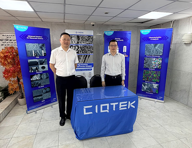
Beyond exhibits, CIQTEK representatives engaged in technical exchange, discussing how advanced SEM tools can bolster regional research infrastructure. We emphasized our commitment to delivering high-performing instruments, competitive pricing, and local support networks to facilitate adoption in diverse labs across the region.
Impact & Outlook
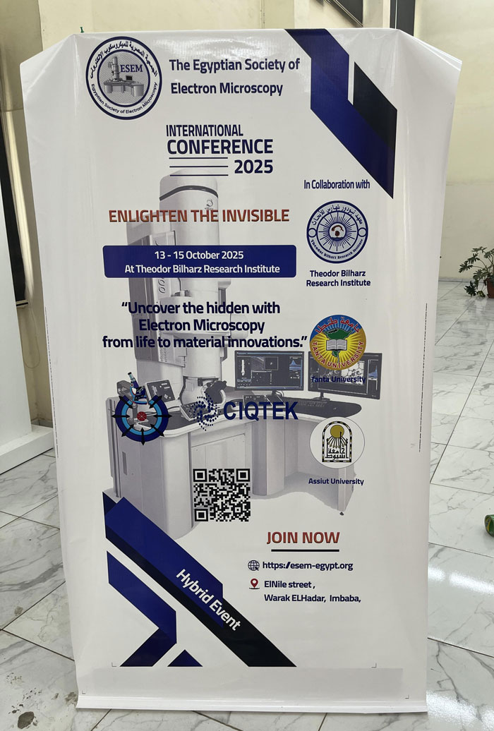
The conference underscored how microscopy continues to unveil the unseen—from cellular ultrastructure to nanomaterial phenomena. For many participants, this was a rare opportunity to access a wide spectrum of imaging techniques under one roof, and to converse directly with vendors like CIQTEK.
By engaging with local scientists and institutions, CIQTEK deepens its global reach and contributes to the growth of microscopy in underrepresented regions. We look forward to continuing our support in Africa and the Middle East through instrument installations, training, and responsive service.
WAIN High-Temperature Series Connectors are certified in accordance with the DIN EN 60 664 / DIN EN 61 994 standards.
Product Advantages
01
High Reliability
Even in extreme temperature fluctuations, WAIN high-temperature series connectors provide stable power transmission and signal conduction.
02
Long Service Life
Made from high-quality materials and rigorously tested, WAIN high-temperature connectors have a long service life, reducing maintenance costs.
03
Strong Applicability
Whether exposed to continuous high temperatures or transient temperature rises, WAIN high-temperature connectors operate normally and are suitable for a variety of complex applications.
04
High Safety
With an IP65/IP67 protection rating, WAIN high-temperature connectors further enhance safety during use.
Technical Parameters
Number of Contacts:6,10,16,24
Rated Current:16A
Rated Voltage:500V
Rated Pulse Voltage:6kV
Contact Resistance:≤1mΩ
Wire Gauge:0.75-2.5mm²(18-14AWG)
Shell Protection Rating:IP65/IP67
Mating Cycles:≥500
Temperature Range:-40℃~+200℃
Contact Material:Copper Alloy
Connection Type:Screw Connection
Contact Plating: Gold/Silver Plating
Insulation Material:LCP
Sealing Component:FPM
Shell Material:Die-Cast Aluminum
All components of the WAIN high-temperature series connectors (including contacts, inserts, shells, seals, and grounding elements) are designed using high-temperature resistant materials, ensuring the product can operate stably within the specified temperature range.
·END·
WAIN is not only manufacturing, but also creating!
Any questions and ideas related to industrial connectors,
You want your home to look bright and stylish. Magnetic track lighting helps make your home feel comfortable. This lighting fits well in modern homes because it looks neat and simple. You can move the lights to shine where you want. This means you can change your room without much work.
Here’s a quick look at how magnetic track lighting is different from regular pendant lighting:
Advantage
Description
Flexible adjustment
You can easily point each light where you want.
Easy to replace fixtures
You can swap out light modules without changing everything.
Versatility
You can mix different lights on one track for more choices.
Change configuration
You can move or change fixtures anytime for a new look.
High safety
Low voltage makes it safer than old high-voltage systems.
Fashionable design
Simple style matches what is popular now.
You save money because these lights use less energy. Magnetic track lighting uses LED technology, so your electricity bill can be up to 60% lower. These lights meet green building rules, so you help the planet while lighting your home.
Tip: If you want your home to look new and modern, magnetic track lighting gives you style and saves money.
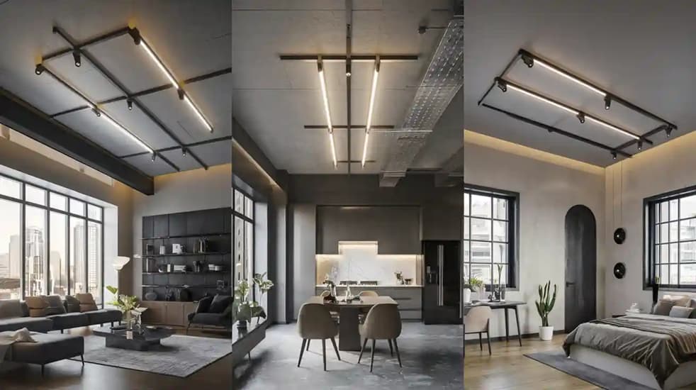
Flexible Installation
Magnetic track lighting is easy to install and does not cause stress. You do not need to worry about lights that cannot move. The modular design lets you adjust and move lights without special tools. You can make your own layout and change it when you want.
Here’s how magnetic track lighting is different from fixed lighting:
Feature
Magnetic Track Lighting
Fixed Lighting Solutions
Installation Flexibility
High – you can adjust lights easily
Low – changes need tools
Repositioning
You can move fixtures without tools
Fixtures stay in one place
Customization
Layouts are easy to change
Layouts are hard to change
Suitable Environments
Homes, offices, galleries
Mostly places that do not change
You can use magnetic track lighting in many rooms, like living rooms, kitchens, or offices. The installation is quick, but you should plan your lighting first. Sometimes, installers make mistakes if they do not know what to do. It helps to plan your installation time, especially if you are fixing up your home.
With magnetic track lighting, you get lights that save energy, are easy to install, and look modern. You can enjoy a system that changes as your needs grow.
Comparing Top-Tier Magnetic Track Lighting Manufacturers
When you look for magnetic track lighting, you want to know which brands are best. You care about how much it costs, how good it is, how it looks, and if it has smart features. Let’s see what top magnetic track brands offer so you can pick the right one for you.
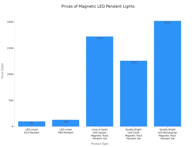
Price and Value
You might ask how much you need to pay for good magnetic track lighting. Prices are different for each brand and model. Some magnetic LED pendant lights start at $49. The most expensive sets can cost more than $2,000. The price depends on the materials, design, and features.
Product Type
Price
LED Linear ECO Pendant
$99
LED Linear PRO Pendant
$129
Lines & Spots – LED Square Magnetic Track Pendant Set
$1,723
Quietly Bright – LED Circle Magnetic Track Pendant Set
$1,259
Quietly Bright – LED Rectangular Magnetic Track Pendant Set
$2,021
LED Pendant Fixtures
From $49
If you want simple lights for a small room, you can find cheaper options. If you want fancy designs or need lights for a business, you might buy the more expensive ones. Usually, better quality and more choices come with a higher price.
Tip: Think about how long you want your lights to last. Paying more now can mean you do not have to replace them soon.
Design and Functionality
Design is important when picking magnetic track lighting. Top brands use strong materials like aerospace-grade aluminum for their best models. This helps the lights stay cool and last longer. Cheaper models use plastic, which may not look as nice or last as long.
Feature
Premium Models
Budget Models
Housing Material
Aerospace-grade or extruded aluminum
Cheaper plastics
Durability
High durability and better heat dissipation
Reduced longevity
Aesthetic Appeal
Enhanced aesthetics due to quality materials
Lower aesthetic value
Premium systems give you more choices. You can pick spotlights, pendants, wall washers, and floodlights. You can mix them to make your own design. Budget systems usually have only basic spotlights, so you have fewer ways to be creative.
Premium magnetic track lighting gives you:
More types of lights for different looks
Stronger materials for better quality
Sleek finishes that fit modern homes
Budget systems give you:
Simple spotlights
Basic designs
Lower price but fewer choices
Some sets, like Lines & Spots, use LED technology and come in black or white. You can change the height and install them easily. This makes them good for homes and businesses. You can make your own lighting style.
Note: If you want your lights to look great and last long, pick a brand that uses good materials and modern designs.
Smart Features (RF, Zigbee, etc.)
Smart features make magnetic track lighting even better. Many top brands now have LED pendant lights with smart controls. You can use your phone, a remote, or your voice to change the lights. Some systems work with Zigbee 3.0 or 2.4G, so you can use them with your smart home.
Product Name
Smart Feature
Compatibility
MiBoxer foldable magnetic black track lighting
Zigbee 3.0
Yes
MiBoxer TS2-30W-ZR dual white modern track lighting
Zigbee+2.4G
Yes
With smart magnetic track lighting, you can:
Change how bright or warm the lights are
Set times for your lights to turn on or off
Control your lights from anywhere in your house
Connect your lights to other smart devices
Some brands have built-in transformers so you can change the hanging height. You get a clean look without extra wires. These smart lights work well in homes and businesses. You can set up different lighting scenes for any mood.
Tip: If you want easy control and lights that work with new tech, choose magnetic track lighting with smart features like Zigbee or RF.
When you compare magnetic track brands, you see big differences in price, quality, design, and smart features. Think about what is most important for your home or business. The right lights can make your space look better, save energy, and feel more comfortable.
Best Magnetic LED Pendant Light Models
Choosing the right pendant light can change the look and feel of your home. You want a model that fits your style, works well, and lasts a long time. Let’s look at some top models from leading brands. Each one brings something special to your space.
FLOS Architectural Model
If you want a pendant light that stands out, you should check out the FLOS Architectural model. This brand is famous for its modern design and smart features. You get a sleek look with strong performance. The FLOS model uses magnetic track lighting to give you flexibility and style.
Here’s a quick look at what makes this model special:
Feature
Details
Light Source
LED
Power
15W/m
Light Temperature
3000K - 1550 lm/m, 4000K - 1660 lm/m
Dimmable
Yes (remote)
Beam Angle
114°
Dimensions
Length: 300/600/900/1200 mm, Height: 15 mm, Depth: 5 mm
Color Rendering Index (CRI)
90
Material
Aluminum
Degree of Protection
IP20
Warranty
2-year warranty from date of purchase
You can adjust the brightness with a remote. The high CRI means colors look true and natural in your room. The aluminum body keeps the light cool and strong. FLOS gives you a clean finish that matches modern homes. You get a two-year warranty, so you know the brand stands behind its product.
Tip: If you want the best magnetic track lighting systems, FLOS Architectural offers a mix of style, quality, and smart controls.
KLUS Design Model
KLUS Design is a brand that focuses on energy efficiency and durability. You get a pendant light that saves power and lasts for years. The led technology in KLUS models converts almost all energy into light, so you waste less electricity. This means lower bills and a smaller carbon footprint.
You can expect these lights to work for 50,000 to 100,000 hours. You do not have to worry about replacing bulbs often. KLUS lights can handle shocks, vibrations, and changes in temperature. You can use them in many places, like kitchens, offices, or living rooms. The design is simple but strong, so it fits many styles.
If you want magnetic track lighting that is easy to install and maintain, KLUS Design gives you a smart choice. The brand is known for making products that last and help you save money.
Note: KLUS Design models are perfect if you want reliable lighting and care about energy savings.
Lodes Model
Lodes is a brand that brings bold design and bright colors to your home. You get pendant lights that catch your eye and make your space feel fresh. Lodes uses led technology to give you strong, clear light. The magnetic track lighting system lets you move and adjust the lights as you like.
You can choose from different shapes and finishes. Lodes models work well in living rooms, dining areas, or even offices. The brand pays attention to detail, so you get a product that looks good and works well. If you want a pendant light that stands out, Lodes is a great pick.
Key features you’ll love:
Unique shapes and colors
Easy adjustment with magnetic track lighting
High-quality led for bright, even light
Durable materials for long-lasting use
Lodes is one of the brands that always tries new ideas. You get a mix of style and function in every model.
Mi-Light Model
Mi-Light is a brand that focuses on smart features and easy control. You can use your phone or a remote to change the lighting in your room. Mi-Light models use led technology for energy savings and bright light. The magnetic track lighting system lets you move fixtures without tools.
You can set timers, adjust brightness, and even change the color temperature. Mi-Light works well with smart home systems, so you can connect your lights to other devices. The design is simple and modern, making it easy to fit in any room.
Why choose Mi-Light?
Smart controls for easy use
Flexible magnetic track lighting
Energy-efficient led
Affordable options for every budget
Mi-Light is one of the brands that makes smart lighting simple. You get good value and lots of features without spending too much.
Tip: If you want smart lighting that is easy to use, Mi-Light gives you control and flexibility.
Quality and Performance
Build Quality
When you pick magnetic LED pendant lights, you want them to last. Good build quality helps the lights work well and stay strong. Top brands use aluminum for the main body. Aluminum makes the fixture tough and helps control heat. This helps the light work better and last longer. Most lights come in black or white powder-coated finishes. These finishes look nice and fit modern rooms.
Many high-quality lights use frosted glass or acrylic parts. These parts spread the light softly and evenly. Some models have a two-way emission system. This means light shines up for a cozy feel and down for tasks. You can see quality in every part, like the mounting kit and safety buckle. These keep the lamp safe and secure.
Here’s what you get with top build quality:
Feature
Details
Material
Durable aluminum construction
Finish Options
Powder-coated black or white
Includes
Mounting kit for suspension
Dimming Options
TRIAC, DALI, and 1-10V
Applications
Residential and commercial spaces
Personalized Control
Adjustable brightness
Design
Modern and architectural
You can trust these brands because they use high standards. Your lights will work well and stay efficient for years.
LED Efficiency
You want lights that save energy and work great. Magnetic LED pendant lights are very efficient. Most models use advanced LED arrays. These turn almost all power into light, not heat. You get more brightness and use less energy.
Let’s look at some numbers. A typical magnetic LED pendant light gives 70 lumens per watt. If you use a 35-watt fixture, you get about 2,450 lumens. This is enough to light a big room and keep your energy bill low.
LED magnetic lights last longer than other lights. Most LED lights can last up to 50,000 hours or more. You do not need to change bulbs often or worry about fixing them.
You help the planet by using efficient lights. High efficiency means less waste and fewer replacements. You save money and help the environment.
Why do people like magnetic LED pendant lights for efficiency and performance?
Lower energy bills
Less heat output
Long-lasting performance
Fewer bulb changes
The long life of LED magnetic lights saves you money and reduces waste because you do not need to replace them often.
When you choose lights with top efficiency and performance, your home feels bright, modern, and smart.
Choosing the Right Magnetic LED Pendant Light
Style and Application
You want your home to look nice and feel cozy. Magnetic LED pendant lights give you many style choices. You can use these lights in dining rooms, living rooms, kitchens, or bedrooms. You can change the height and position to get a new look. These lights are both pretty and useful, so they stand out in any room.
Magnetic pendant lights hang from tracks. You can move them to shine on a kitchen island or dining table. The hanging style makes the room look interesting. The magnetic part lets you adjust the lights easily. If you want a comfy reading spot or new bedside lamps, these lights work well. You can also use more than one light to make your living room or bedroom feel balanced.
Here’s a simple guide for matching lights to each room:
Room Application
Recommended Color Temperature
Placement Tips
Kitchen
4000K to 5000K (bright white)
Hang 30-36 inches above countertop
Dining Room
3000K (warm white)
Hang about 30 inches above table
Living Room
Dimmable options for ambiance
Varies based on activity
Bedroom
Layered lighting with flexibility
Position based on needs
You can choose energy-saving lights for every room. These options help you use less power and keep your home bright.
Budget Considerations
You want good lights but do not want to spend too much. When you shop for magnetic LED pendant lights, look at both price and quality. Some brands use strong LED chips like Cree or OSRAM. These chips last longer and shine brighter. The paint finish is important too. Special spraying makes the lights smooth and helps them last.
Accessories like plugs and covers help your lights stay strong. Good power supplies with warranties are important. Cheaper lights might not last long or work well. Sometimes, big brands cost more because they spend money on ads, not just quality.
Here’s a table to help you balance price and quality:
Factor
Description
Quality of LED chips
Better chips mean longer life and brighter lighting
Paint spraying process
Smooth finish lasts longer
Quality of accessories
Good plugs and covers add durability
Power supply options
Reliable supplies keep your lighting safe
Brand premiums
Higher prices may include advertising costs
If you want to save money, pick energy-saving lights. These lights use less power and last longer, so you spend less over time. You can find styles and features that fit your budget and still get great lights for your home.
You have lots of choices for magnetic LED pendant lights. FLOS, KLUS, Lodes, and Mi-Light give you great lighting for homes and commercial spaces. You can pick lighting that fits your style and budget. If you want commercial magnetic lighting solutions, these brands offer strong commercial lighting for offices and shops. Good lighting makes your space look better. You can visit manufacturer websites or talk to lighting experts for help with commercial lighting. Smart features and strong design help you get the best commercial lighting for every room.
Tip: Try different lighting setups to see what works best for your commercial needs.
You can elevate your kitchen island with an S-shaped curvy magnetic track. This design brings a sense of movement and sophistication to your home. The track follows the contours of your island, creating a visual centerpiece that draws attention. You achieve balanced lighting across the entire surface, making food preparation and entertaining easier. The flexibility of the track allows you to adapt the layout to any kitchen shape, whether you have a straight or curved island.
An S-shaped track lets you position lights exactly where you need them. You can highlight decorative elements, such as countertops or bar stools, with focused illumination. The magnetic system makes installation simple, so you can update your lighting as your design preferences change. You create a dynamic atmosphere that enhances both function and style.
Tip: Use an S-shaped track to break up straight lines in your kitchen and add visual interest to your home.
Task and Accent Light
You need effective task lighting for your kitchen island. Curvy magnetic track lights provide targeted illumination for chopping, cooking, and serving. You can adjust each light to focus on specific areas, ensuring you have enough brightness for every activity. The track system supports both task and accent lighting, so you can combine practical illumination with decorative effects.
Accent lights help you showcase design features, such as a unique backsplash or stylish cabinetry. You can use the track to create layers of lighting, blending ambient and focused illumination for a professional look. The magnetic installation allows you to reposition lights easily, adapting to new design trends or changes in your home layout.
Lighting Type
Purpose
Benefit
Task Lighting
Food prep
Clear, bright illumination
Accent Lighting
Decorative focus
Highlights design details
You achieve a modern kitchen atmosphere by integrating curvy magnetic track lights. The combination of S-shaped track layouts and adjustable fixtures ensures your home stands out with both beauty and functionality.
Flowing Ceiling Lines
You can create a striking visual impact in your living room by installing curvy magnetic track lighting along the ceiling. The track follows the architectural lines, guiding lights in smooth, uninterrupted paths. This approach allows you to highlight the unique structure of your home and draw attention to specific areas. You achieve a modern look that feels both dynamic and inviting. Magnetic track lighting adapts to any ceiling shape, whether you have gentle curves or bold waves. You position lights to accentuate artwork, furniture, or decorative elements. The flexibility of the track system lets you change the arrangement as your style evolves. You enhance the overall illumination, making your living room feel brighter and more spacious.
Tip: Use flowing track layouts to connect different zones in your living room, creating a sense of movement and unity.
You maximize the use of available space by letting the track lighting follow the natural contours of your ceiling. This technique helps you avoid harsh shadows and ensures even illumination throughout your home. You can combine ambient and accent lights for a layered effect that elevates the atmosphere.
Layered Effects
You achieve a sophisticated ambiance in your living room by using layered lighting with curvy magnetic track systems. Layered illumination involves combining multiple types of lights, such as ambient, accent, and task lighting, to create depth and dimension. You control the mood and functionality of your space with this approach. Magnetic track lighting gives you the freedom to adjust each fixture, tailoring the brightness and direction to suit your needs.
Consider the following benefits of layered lighting effects in your living room:
Benefit
Description
Modern Design
Curvy magnetic track lights integrate well into various spaces, enhancing the aesthetic appeal.
Flexibility
These lights can create both independent and interactive areas, promoting relaxed communication.
Emotional Atmosphere
Comfortable color options help in creating a personalized emotional atmosphere.
You use track lighting to define separate zones for reading, entertaining, or relaxing. You select color temperatures and brightness levels that match your desired ambiance. The magnetic system allows you to reposition lights easily, adapting to changes in your home layout. You create a welcoming environment that supports both social gatherings and quiet moments.
Note: Layered track lighting not only improves illumination but also adds visual interest and emotional warmth to your living room.
Headboard Curves
You can transform your bedroom into a sanctuary by installing a curvy magnetic track above or around your headboard. This approach allows you to create a focal point that draws the eye and adds a sense of luxury to your home. The track bends smoothly to follow the shape of your headboard, whether you prefer gentle arcs or bold waves. You gain full control over the placement of your lights, ensuring that every part of your bed receives the right amount of illumination.
A well-designed track system lets you highlight textures and colors in your bedding or wall art. You can use accent lighting to showcase decorative pillows or unique headboard materials. The flexibility of the track means you can change the arrangement as your style evolves, keeping your bedroom lighting fresh and modern. By integrating the track into your bedroom design, you create a seamless look that enhances the overall atmosphere of your home.
Tip: Position your track to create a halo effect above the headboard for a soft, inviting glow that encourages relaxation.
Soft, Relaxing Light
You set the mood for restful sleep by choosing soft, relaxing lighting in your bedroom. Strategic lighting design plays a crucial role in supporting healthy sleep patterns. Poor lighting can disrupt your circadian rhythm, making it harder to unwind at night or feel refreshed in the morning. By using a curvy magnetic track, you can install lights that mimic natural light cycles—bright during the day and gentle as bedtime approaches.
Bright lighting, especially blue light from screens, can reduce melatonin production, which is essential for sleep.
Exposure to cool, intense light in the evening signals your body to stay awake, making it difficult to relax.
Gradually dimming your lights and selecting warm-colored bulbs creates a soothing environment that helps you wind down.
A magnetic track system allows you to adjust the direction and intensity of your lights with ease. You can create layers of illumination, combining ambient and accent lighting for a balanced effect. This approach ensures your bedroom feels comfortable and inviting, supporting both relaxation and rejuvenation. By prioritizing soft lighting, you enhance the quality of your sleep and elevate the ambiance of your home.
Room Dividers with Magnetic Track Rail Lighting System
You can transform an open-plan area by using a magnetic track rail lighting system as a visual room divider. This approach allows you to define boundaries without building walls. The track follows the lines of your space, guiding lights along the ceiling or even down vertical surfaces. You create distinct zones for dining, relaxing, or working, all while maintaining an open feel in your home.
A magnetic track rail lighting system offers unmatched flexibility. You can reposition lights to highlight specific features or adjust the track layout as your needs change. The system adapts to any room shape, curving around furniture or architectural elements. You achieve clear separation between zones, yet keep the overall design cohesive. The magnetic track rail lighting system also supports layered lighting, so you can combine ambient and accent lights for optimal illumination.
Tip: Use the magnetic track rail lighting system to frame a reading nook or workspace, making each area feel intentional and inviting.
Light Patterns for Zones
Strategic lighting patterns help you create functional and beautiful zones in open spaces. You can use a magnetic track rail lighting system to direct light where you need it most. Positioning the track near floor-to-ceiling windows or skylights maximizes natural light, while reflective surfaces amplify brightness and improve energy efficiency. Large glass panes establish a visual connection with the outdoors, enhancing the sense of openness in your home.
Place key areas, such as seating or workspaces, near windows to take advantage of daylight.
Use the magnetic track rail lighting system to manipulate light and shadow, defining each zone with precision.
Select different track layouts for each area, such as curves for relaxation zones and straight lines for workspaces.
Incorporate the magnetic track rail lighting system to layer lights, blending ambient and task lighting for balanced illumination.
Lighting serves as a source of energy, shaping the atmosphere in every part of your home. By using the magnetic track rail lighting system, you control the mood and function of each zone. You create a harmonious flow between spaces, ensuring every area receives the right amount of illumination and style.
Following Stair Paths
You can elevate your staircase with a curvy magnetic track system. The track follows the path of your stairs, creating a continuous line of lighting that guides movement. You achieve a seamless look by installing the track along the wall or ceiling, matching the curve or angle of each step. This approach transforms your staircase into a design feature within your home. You position lights at strategic intervals to ensure consistent illumination from the bottom to the top. The magnetic track allows you to adjust the placement of lights, adapting to changes in your home’s layout or style.
Tip: Place the track on both sides of the staircase for balanced lighting and enhanced visibility.
Consider these benefits when you use a curvy magnetic track for your staircase:
You create a safe passage with clear illumination.
You highlight architectural details, such as railings or decorative steps.
You add a modern touch to your home’s interior.
Feature
Track Lighting Benefit
Curved staircases
Flexible track installation
Landings
Layered illumination
Narrow steps
Adjustable lights
Safety and Style
You improve safety and style by integrating curvy magnetic track lighting on your staircase and landing. The track provides focused illumination, reducing shadows and making each step visible. You minimize the risk of accidents, especially in homes with children or elderly residents. The magnetic system lets you reposition lights to target high-traffic areas or dark corners. You select fixtures that complement your home’s décor, blending function with aesthetics.
You can use layered lighting to create a welcoming atmosphere on landings. The track supports both ambient and accent lights, allowing you to highlight artwork or architectural features. You achieve a cohesive look by matching the track design with other lighting elements in your home. The flexibility of the magnetic track system ensures your staircase remains both safe and stylish.
Note: Smart controls let you adjust the brightness of your lights, providing optimal illumination for every time of day.
You transform your staircase and landing into standout features by using curvy magnetic track lighting. You combine safety, style, and modern design to enhance your home’s overall appeal.
Bold Curves
You can make a powerful first impression by installing a curvy magnetic track in your entryway. The track bends with confidence, guiding the eye from the front door into the heart of your home. When you select bold curves, you introduce a sense of movement and energy. This design choice sets the tone for the rest of your space. You can use the track to highlight architectural features, such as arches or textured walls, and create a visual path that welcomes guests.
A well-placed track system allows you to layer lighting for both function and style. You can position lights to eliminate shadows and ensure even illumination. The flexibility of the track means you can adapt the layout as your style evolves. You achieve a seamless blend of aesthetics and practicality. Consider these benefits when you choose bold curves for your entryway:
Draw attention to unique design elements
Guide visitors naturally into your home
Create a signature look with custom lighting arrangements
Tip: Use a combination of direct and indirect lights along the track to add depth and dimension to your entryway.
Welcoming Light
You set the mood for your entire home with the right lighting in your entryway. A thoughtfully designed track system provides both brightness and warmth. You can select fixtures that complement your décor and adjust the lights to suit different times of day. The entryway often serves as the first point of contact for guests, so your lighting choices matter.
A thoughtfully designed entryway serves as a prelude to the rest of the home, blending elegance, warmth, and personality. By combining materials, lighting, and functional elements with care, you can create a space that leaves a lasting impression while remaining practical for everyday life.
You can use the track to layer illumination, combining ambient and accent lights for a balanced effect. This approach ensures your entryway feels inviting and safe. You also gain the flexibility to update your lighting as trends change or your needs shift. The magnetic track system supports easy repositioning, so you always maintain optimal illumination.
A welcoming entryway with well-designed lighting not only enhances the beauty of your home but also improves functionality. You create a space that feels both elegant and practical, setting the stage for the rest of your living environment.
Creative Shapes for Focus
You can transform your home office into a productive environment by using curvy magnetic track lighting. The flexibility of the track system allows you to create unique shapes that support focus and creativity. You can arrange the track in straight lines for a clean, modern look or bend it into gentle curves that follow the contours of your workspace. Some people choose complex custom shapes to define specific zones or highlight important areas. These creative arrangements help you direct lights exactly where you need them, reducing distractions and improving concentration.
Straight tracks provide a structured, organized feel.
Curved tracks soften the atmosphere and add visual interest.
Custom shapes can wrap around shelves or frame a desk area.
You can integrate the track with shelves or wood accents to create a cohesive design. When you combine lighting with other elements, you add both function and style to your home office. The ability to reposition lights along the track means you can adapt your setup as your needs change. This approach ensures your workspace always supports your goals.
Tip: Use a curved track above your desk to create a focused pool of illumination that keeps you energized throughout the day.
Productivity Lighting
Effective lighting plays a crucial role in your productivity. You need a system that delivers both ambient and task illumination. Curvy magnetic track lights give you control over brightness and direction, allowing you to tailor the lighting to your workflow. You can position lights to reduce glare on screens and highlight important documents. The track system supports layering, so you can blend general and focused lighting for optimal results.
You can enhance your home office design by selecting fixtures that match your décor. Wood accents or metal shelves pair well with the sleek lines of the track. This combination creates a professional atmosphere that inspires you to do your best work. The flexibility of the track system means you can update your lighting as your projects evolve. You maintain a workspace that feels both modern and comfortable.
A well-designed lighting plan helps you stay alert and motivated. You can use the track to highlight artwork, plants, or organizational tools, making your home office a place where you enjoy spending time. The right illumination supports your productivity and elevates the overall design of your home.
Curvy magnetic track lighting gives you endless ways to brighten and enhance your home. You can spotlight architectural features, customize ambiance, and integrate modern aesthetics with ease:
Key Benefit
Description
Enhancing Architectural Features
Rail lighting excels at spotlighting architectural features and artworks, turning them into focal points that captivate and enhance the viewer’s experience.
Customization for Unique Ambiance
Allows adjustment of fixture placement and direction to create different moods, from soft ambient light to bright task lighting.
Integrating with Modern Aesthetics
Seamlessly fits into modern aesthetics with sleek lines, complementing minimalist spaces while allowing for expressive design.
You can adapt track layouts, rearrange lights, and layer illumination to suit any room. Flexible lighting supports healthy routines, boosts productivity, and elevates your daily environment. Try new ideas, share your creative lighting solutions, or ask questions below—your home deserves standout illumination.
Here’s a quick look at how LED spot lights compare to halogen spot lights:
Light Type
Wattage
Daily Usage
Annual Energy Consumption (kWh)
Energy Savings Compared to Halogen
Halogen Spot Light
50 W
4 hours
73 kWh
N/A
LED Spot Light
10 W
4 hours
14.6 kWh
~80% less energy
Tip: If you want a lighting system that saves money and lasts longer, choose magnetic LED lights.
LED magnetic track lights also help keep your room cool. Old bulbs get hot, but LEDs stay cool. This makes your home safer and more comfortable.
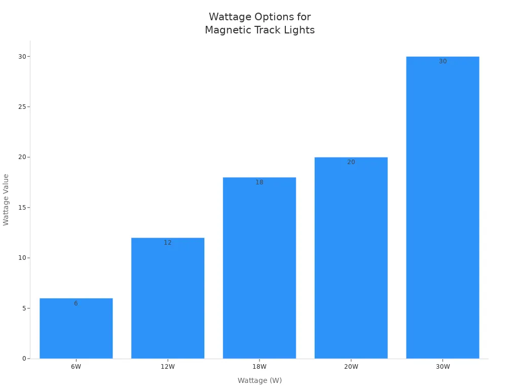
Wattage
Wattage tells you how much power your lights use. Most magnetic track lights for homes come in different wattage options. You can pick the right one for your space. Lower wattage means less energy used, but you still get bright light with LEDs.
Here’s a chart showing common wattage choices for magnetic track lights:
Type of Track Light
Wattage Range
Magnetic Track Lights
6W, 12W, 18W, 20W, 30W
You can mix and match wattages in your recessed magnetic track light. For example, use lower wattage magnetic LED lights for cozy corners and higher wattage for work areas. Always check your track rail compatibility before installation. Some rails work better with certain wattages.
Beam Angles
Beam angle decides how your lights shine in the room. Narrow beam angles (below 30°) focus light on one spot. These are great for reading nooks or art walls. Wider beam angles (above 60°) spread light across the room. You get softer, even lighting for general use.
Narrow beam angles make light more intense in one area.
Wider beam angles cover more space but feel less bright.
Pick your beam angle based on room size, ceiling height, and what you want to light up.
If you want your magnetic track lighting to look good and work well, think about the beam angle during installation. For high ceilings, use narrow beams. For wide rooms, use wider beams.
Dimming Options
Dimming lets you control how bright your lights are. Many magnetic track lights offer dimming features. You can change the mood in your room with just a touch. Dimming also saves energy because you use less power when you lower the brightness.
Here are some popular dimming methods for magnetic track lighting:
Dimming Method
Description
0-10V Dimming
Standard dimming for many lights.
DALI Dimming
Advanced digital control.
Bluetooth
Wireless control with your phone.
Zigbee
Smart home wireless control.
WIFI Dimming
Control lights from anywhere in your house.
Note: Before installation, check if your magnetic LED lights and track rails support dimming. Not all systems work with every dimming method.
Dimming options make your lighting system flexible. You can set the perfect brightness for movie nights, homework, or parties.
Magnetic Track Light Design and Compatibility
You have many choices for magnetic track light design. You can pick linear, L-shape, oval, round, square, or even snake-shaped layouts. Each design fits different rooms and styles. Magnetic track rails come in sizes like 20mm (M20), 35mm (M35), and even slim 15mm tracks. You can install them recessed, suspended, or surface-mounted.
Modular magnetic LED lights let you add, remove, or move fixtures easily.
Always match your magnetic track lighting system with the right rail and power supply.
Make sure your installation fits your room’s needs and electrical system.
If you mix low voltage and line voltage systems, you might damage your equipment. Always check compatibility before you start installation.
Tip: Surface magnetic track lighting uses matte black finishes and sustainable materials. These trends help your home look stylish and save energy.
Types of Magnetic Track Lights
When you look at the different types of magnetic track lights, you’ll see that each one fits a certain space or need. The right choice depends on your room size, ceiling height, and what you want to light up. Let’s break down the most common types of magnetic track lights and where they work best.
Linear
Linear magnetic track lights give you a straight, clean look. You can use them in living rooms, kitchens, or hallways. They spread light evenly across the space, making them great for large open areas. If you want a simple and modern magnetic track light design, linear tracks are a solid pick.
Tip: Linear tracks work well for long spaces. You can highlight a hallway or brighten up a kitchen counter.
Parallel
Parallel track lights use two or more tracks side by side. This setup gives you more coverage and flexibility. You can light up bigger rooms or create zones in open spaces. Parallel tracks fit well in offices, big living rooms, or any place where you need more light.
You can use parallel tracks to focus on different areas at once.
They help you avoid dark corners in wide rooms.
Modular
Modular magnetic track lights give you the most flexibility. You can move, add, or remove lights without tools. This type works well if you like to change your room’s look or need to light up different spots at different times. Modular systems also save energy because they use low voltage.
Feature
Modular Magnetic Track Lights
Linear and Parallel Track Lights
Flexibility
High - easy repositioning and customization
Low - limited adaptability
Energy Efficiency
Operates on low voltage
Operates at line voltage
Customization
Can be extended and shaped
Fixed design
If you want a lighting system that grows with your needs, modular is the way to go. You can shape the tracks to fit any room, big or small.
No matter which type you choose, magnetic track lighting lets you match your lights to your space. Think about your room’s layout and pick the type that fits best.
Magnetic Track Lighting Room Guide
Living Room
The living room is where you relax and hang out. You want the lights to feel cozy and show off special things. Magnetic track lighting gives you many choices for style and saving energy.
Here’s a table with popular magnetic track light setups for living rooms:
Configuration Type
Description
Zigzag Patterns
Makes cool light and shadow shapes, so your room looks fun.
Layered Installations
Uses tracks at different heights, which is great for tall ceilings.
Accent Lighting
Shines on art or cool parts of the room, so people notice them.
You should pick LED magnetic track lights to save energy. Dimmable lights let you change how bright it is for movies or parties. This saves power and helps set the mood.
Tip: If your living room has tall ceilings, try layered tracks. You will get a bold look and more even light.
Kitchen
The kitchen needs bright lights for cooking and cleaning. Magnetic track lighting is good here because you can move the lights around. This helps you get the right light for chopping food or reading recipes.
Magnetic track lighting makes task lighting better in kitchens. You can point magnetic LED lights at counters, sinks, or tables. LED lights use less power than old bulbs, so you save energy every day. If you use dimmable lights, you can make them less bright when you do not need full power.
Note: Always check that your track rails and power supply match before you put them in. This keeps your lights safe and working right.
Bedroom
You want your bedroom to feel peaceful and calm. Magnetic track lighting lets you mix different lights for a nice look. You can use magnetic LED lights for reading, getting dressed, or sleeping.
Here’s how to set up bedroom lighting:
Use different lights for general, task, and accent lighting.
Pick LED fixtures to save money and need less fixing.
Add lights you can move or dim to change the mood.
Choose LED magnetic track lights for easy care and saving energy.
Look for Energy Star labels to make sure you are saving power.
Get a system with dimming so you can change the brightness.
Layered lighting helps you relax and makes your bedroom work better. You can move lights or change how bright they are whenever you want.
Bathroom
Bathrooms need safe and strong lights. Magnetic track lighting works well here, but you must be careful with electricity. Always use a special transformer to change high voltage to low voltage. This makes it safer and lowers the chance of shock.
Make sure all wires are tight and covered.
Check wires and lights often after you put them in.
Magnetic track lighting uses low voltage, which is safer in wet places.
These systems help stop overload and overheating, so fires are less likely.
Alert: Never skip safety checks in the bathroom. Good installation keeps your lights safe and working for a long time.
Hallway
Hallways can feel dark or small. Magnetic track lighting can help by giving you lights you can move and aim. You can point lights at art, doors, or just make the hallway brighter.
Here’s a table showing how magnetic track lighting helps in hallways:
Feature
Benefit
Flexible and Adjustable
Lets you change the lights for your hallway, so you see better.
LED Technology
Uses less power than old bulbs, so you pay less.
Dimming and Motion Control
Lights turn on only when needed, so you save money and energy.
Reconfigurability
You can change the setup, so you always have good lighting without extra cost.
Tip: Use motion sensors with your magnetic track lights. The lights turn on when you walk by and off when you leave, so you save energy.
Home Office
Your home office needs good lights for work and video calls. Magnetic track lighting lets you set up general, task, and accent lights. You can move lights to shine on your desk or shelves.
Here’s a table showing why magnetic track lighting is good for home offices:
Advantage
Description
Easy Installation
You can put in magnetic track lights fast without lots of wires.
High Flexibility
Move lights for different jobs, like reading or typing.
Energy Efficiency
Magnetic LED lights use less power, so you save money.
Aesthetic Appeal
Modern styles make your office look nice and professional.
Sustainability
Many systems use LED technology, which is better for the planet.
You can use magnetic linear lights for general lighting. They spread light evenly and help stop glare. Add magnetic spotlights to shine on important things or art. This setup helps you focus and makes your office look good.
Note: Always make sure your track rails and power supply match before you put them in. This keeps your lights safe and working well.
Energy Consumption Tips
Placement
Where you put your lights matters a lot for energy consumption. If you arrange magnetic track lighting in smart ways, you can light up your room with fewer bulbs. Try to focus your lights on spots where you need them most, like reading corners or kitchen counters. Adjustable fixtures let you point light exactly where you want, so you don’t waste energy lighting empty spaces. Good placement means you get better light and use less power. Before installation, plan your lighting system layout to avoid adding extra lights later.
Tip: Place magnetic LED lights to cover key areas. You’ll save energy and get the right brightness.
Maintenance
Keeping your lighting system in good shape helps lower energy consumption. You should check your lights often to make sure everything works right. Clean the fixtures and tracks so dust doesn’t block the light or trap heat. Look for loose wires or weak connections during installation and after. Regular care keeps your lights bright and safe.
Inspect all parts of your lighting system.
Clean lights and tracks to boost light output.
Make sure wires and connections stay tight.
Sensors and Timers
Smart controls like sensors and timers can cut down energy use. Sensors turn lights on when you enter a room and off when you leave. Timers let you set when lights should run, so you don’t forget to turn them off. Some lighting systems use AI-driven sensors for even better control. These features help you use only the energy you need. In places like malls, sensors have saved up to 35% on energy consumption. You can also adjust brightness and color with smart controls, making your lighting system work for you.
Note: Always use bulbs that match your system and avoid overloading the power supply during installation.
Mistakes to Avoid
Overloading Power Supply
Adding more lights might seem like a good idea, but it can cause problems if you use too many. If you mix parts from different brands, they might not work well together. Using too many lights or going over the wattage limit can make your system get too hot. Watch for lights that flicker or breakers that turn off. These are signs your magnetic track lighting has too much power. Always check the total wattage before you put in your lights.
Using different brands can make things not fit right.
Too many lights or high wattage can make things too hot.
Flickering lights or breakers turning off mean you should check your system.
Tip: Use the same brand for your magnetic track light system and never use more wattage than allowed.
Ignoring Room Needs
Each room in your house needs its own kind of lighting. If you don’t think about this, some rooms might be too dark or too bright. This can make your rooms feel bad and use more energy. You might add extra lights or use bulbs that are too strong.
Every room needs different lights for its size and use.
Not thinking about this can waste energy and give you bad lighting.
Magnetic track lighting works best when you set it up for each room.
Note: Plan your lighting for every room so you get the best light.
Neglecting Maintenance
If you don’t check your lights often, they can get dim or stop working. Dust and loose wires can be dangerous. Here’s what can happen if you forget to take care of your lights:
Consequence
Description
Reduced lighting performance
Your lights might not be as bright or even.
Safety hazards
Loose wires can start electrical fires.
Potential system failures
The whole lighting system could stop working.
Tip: Clean your magnetic LED lights and check the wires often to keep them safe and bright.
Choosing Style Over Efficiency
It’s easy to pick lights that look cool, but you should also think about how much energy they use. Some stylish lights don’t save energy, so your bills go up. Magnetic track lighting with LED technology can save you up to 80% on energy compared to old lights. Even if fancy lights cost more at first, you save money later with efficient lighting.
Aspect
Description
Energy Efficiency
LED magnetic track lighting helps you pay less for energy.
Initial Cost
Trendy lights might cost more and not save energy.
Long-term Savings
Efficient systems save you money and need less fixing.
Note: Pick lights that look nice and save energy for the best results.
When you choose magnetic track lighting, remember these tips. Think about what each room needs to feel and work right. Always check load capacity and fixture compatibility for safety. Pick LED lights that save energy and use the correct voltage.
Benefit
Description
Energy Efficiency
LEDs use less power and last a long time.
Flexibility
You can put lights where you need them most.
Low Heat
LEDs help keep your rooms cooler.
Make good choices so you can enjoy great lighting in every room!
From the Politecnico di Milano to the National Research Council (CNR) and major materials institutes in Emilia-Romagna, SEM has become indispensable for both academic and industrial research. Italian laboratories rely on these systems to study metals, ceramics, semiconductors, biological samples, and even ancient artifacts.
Recent years have seen a shift from conventional tungsten SEMs to field emission SEM (FE-SEM) platforms, which deliver higher spatial resolution and more stable imaging performance. This evolution reflects the country’s growing focus on nanostructured materials, energy devices, and precision manufacturing — all areas where nanoscale imaging and analysis are crucial.
Performance Priorities for Italian SEM Users
Italian researchers tend to emphasize several practical factors when evaluating SEM systems:
Resolution and imaging stability: The ability to observe nanoscale details in materials such as thin films, catalysts, and nanocomposites.
Analytical integration: Compatibility with EDS, EBSD, and WDS systems to extract chemical and crystallographic information alongside morphology.
Ease of operation and automation: Software-guided imaging and recipe-based workflows are increasingly preferred in multi-user facilities.
Temperature and environmental control: In-situ observation of microstructural evolution under heating or vacuum changes is becoming more common.
Service and long-term support: Access to local technical expertise and responsive maintenance is a key factor in supplier selection.
These priorities reflect a broader trend: Italian laboratories are modernizing not only their instrumentation but also their workflow efficiency and data reliability.
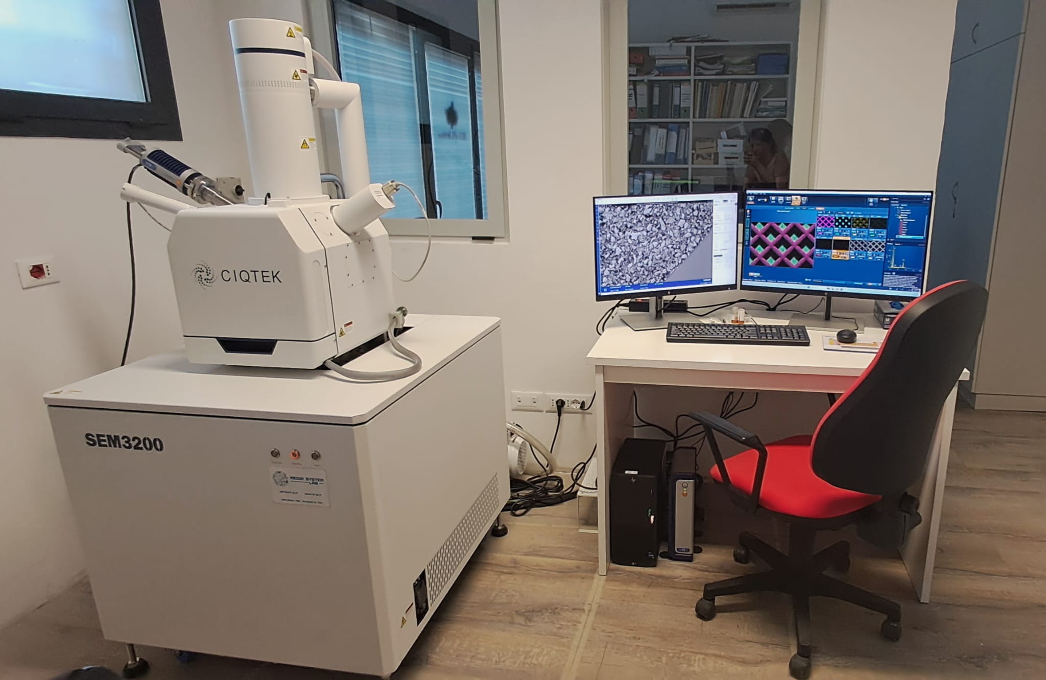
Modern SEM Systems Entering the Italian Market
In recent years, CIQTEK’s SEM instruments have been increasingly adopted by research and industrial users across Italy. Several systems, including the SEM3200 and SEM3300, have been installed through CIQTEK’s local partner in Rome. It has also established a dedicated CIQTEK SEM demonstration laboratory, where Italian researchers can experience the imaging performance and analytical capabilities of the systems firsthand. These installations highlight the country’s growing interest in high-resolution, stable, and user-friendly SEMs supported by local expertise.
A Growing Ecosystem for Advanced Electron Microscopy
Italy’s strong tradition in materials and applied sciences continues to drive demand for advanced electron microscopy. National research centers, universities, and technology companies are jointly shaping a dynamic environment where innovation in imaging and analysis thrives.
With more international suppliers now offering localized support and demonstration facilities, such as CIQTEK’s growing presence through its partner network, Italian users have access to an expanding ecosystem of high-performance, reliable SEM solutions. In addition to advanced imaging quality and stable performance, CIQTEK SEM systems are recognized for their competitive pricing, making high-end field emission microscopy more accessible to a wider range of research and industrial users.
This growing accessibility, combined with strong local technical support, ensures that Italy remains at the forefront of microscopy research and application in Europe, where precision, performance, and affordability converge to empower the next generation of scientific discovery.
The new setup allows researchers and industrial users in Europe to experience high-resolution imaging, analytical performance, and ease of operation offered by the CIQTEK SEM4000Pro. The system provides outstanding image quality for fine microstructural observation and supports a wide range of applications in materials science, microelectronics, and R&D.
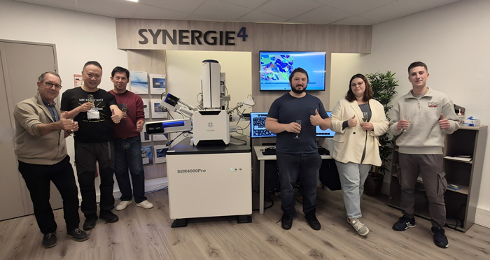
SYNERGIE4 is CIQTEK's French distributor and service provider for advanced microscopy and microanalysis solutions. With extensive experience in electron microscopy and analytical instruments, SYNERGIE4 supports universities, research institutes, and industrial labs across France with tailored solutions, technical expertise, and training.
Now, SYNERGIE4’s demo center features a fully operational CIQTEK SEM4000Pro, offering hands-on demonstrations for visitors to explore its imaging capabilities, intuitive software interface, and versatility across various research fields.
“Having the CIQTEK SEM4000Pro available in our showroom allows us to showcase its imaging performance directly to our customers,” said a representative from SYNERGIE4. “It’s a great addition to our demonstration facilities and an important step in expanding our microscopy portfolio.”
With the SEM4000Pro now available in France, European users can directly evaluate its performance, supported by SYNERGIE4’s local expertise and technical demonstration services. This collaboration marks a significant milestone in CIQTEK’s ongoing effort to enhance accessibility to advanced electron microscopy technologies across Europe.
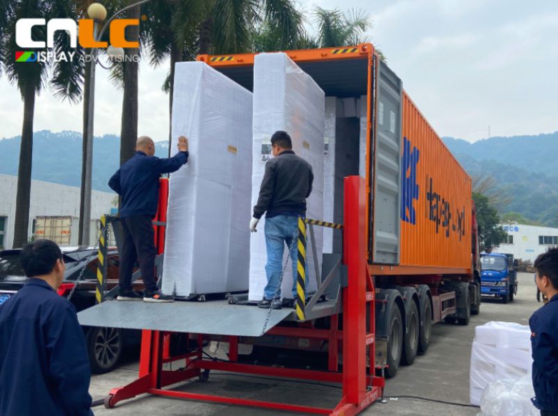
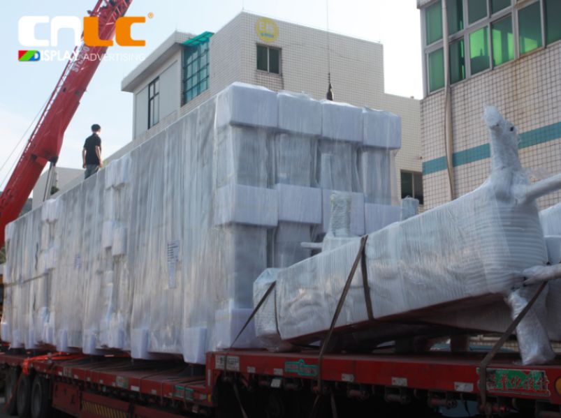
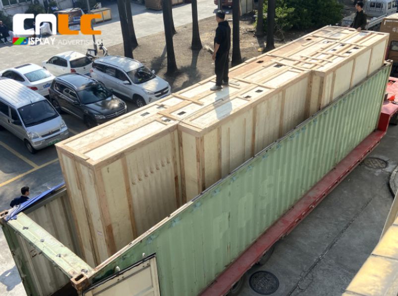
1. CBU – Completely Built-Up: The Turnkey Solution
The CBU model is ideal for clients who need ready-to-install products with zero technical complexity. CNLC provides fully assembled LCD displays, LED screens, and light box solutions that meet global standards for durability, brightness, and outdoor performance.
Who Chooses CBU?
Global distributors who prioritize speed and convenience
Retail solution providers needing plug-and-play digital signage
Projects requiring small-batch customization with short lead times
Key Benefits of CBU
✔ Complete product delivered, ready for immediate installation ✔ Superior quality control under factory conditions ✔ Optional custom designs for unique branding or project needs
Example Use Case: A retail chain launching 50 stores across Europe needs consistent, high-quality digital signage delivered within a tight timeline. The CBU model ensures uniform standards and rapid deployment.
2. SKD – Semi Knocked Down: The Smart Balance
The SKD model is a popular choice for system integrators, engineering companies, and regional assembly partners. Under SKD, CNLC provides the structural framework, housing, and key mechanical parts, while the client sources specific components—such as LG LCD panels or specialized LED modules—locally.
Why SKD?
Reduces shipping costs due to optimized packaging
Helps minimize import duties in certain regions
Offers flexibility in component selection
Best For:
✔ Businesses with basic assembly capabilities ✔ Companies seeking cost-efficiency without compromising quality ✔ Markets where local labor and parts are affordable and accessible
Example Scenario: A digital signage integrator in the Middle East sources LG LCD panels locally while importing SKD kits from CNLC. This approach saves on logistics and complies with local regulations.
3. CKD – Completely Knocked Down: Maximum Control for OEMs
The CKD model is designed for OEM partners and local manufacturers who aim to establish full-scale assembly operations in their home country. CNLC supplies all components, along with technical documentation, assembly training, and production support.
CKD Package Includes:
✔ Complete component sets ✔ Assembly guides and engineering support ✔ Optional on-site training for local teams ✔ Assistance with machinery setup and quality assurance
Advantages:
Enables full local manufacturing
Reduces overall logistics and tariff costs
Ideal for large-scale or long-term projects requiring local compliance
Example: A partner in South America sets up a factory to assemble 1,000 units annually using CKD kits from CNLC. This model maximizes cost efficiency and strengthens their local supply chain.
How to Choose the Right Model for Your Business?
Model
Assembly Level
Ideal For
Key Benefit
CBU
Fully Assembled
Distributors, retailers
Plug-and-play solution
SKD
Semi-Assembled
Integrators, engineering firms
Cost savings & flexibility
CKD
Fully Disassembled
OEMs, factories
Local production & scalability
Why CNLC?
With over 18 years of experience in the display industry, CNLC specializes in high-brightness LCD digital signage, LED billboards, and outdoor light box solutions. Our manufacturing facilities in Guangzhou use precision-molded aluminum structures and cutting-edge technology to deliver durable, customizable, and globally compliant products.
When you partner with CNLC, you gain:
Flexible delivery models tailored to your business
Expert engineering support for seamless integration
Proven global experience across Europe, the Middle East, and North America
Conclusion
Choosing between CBU, SKD, and CKD depends on your business size, market strategy, and operational capabilities. CNLC is here to help you select the most efficient solution, whether you need a turnkey system, semi-assembled kit, or a full OEM component package.
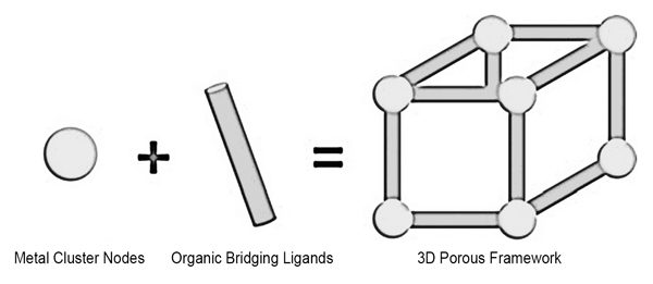 Figure 1. Schematic of a Metal–Organic Framework
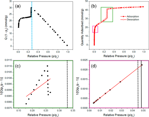 Figure 2. (a) Rouquerol plot indicating correct data points (left of dashed line); (b) N₂ adsorption/desorption isotherms showing intervals used for BET plots c (green) and d (pink); (c, d) BET plots with p/p₀ ranges 0.17–0.27 and 0.004–0.05, respectively. Solid lines correspond to n(m) at p/p₀ (Rouquerol criterion iii), dashed lines correspond to 1/√C + 1 (criterion iv).
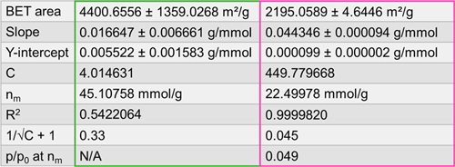 Table 1. BET areas, slopes, intercepts, C constants, monolayer capacities n(m), R², 1/√C + 1, and corresponding p/p₀ values for plots c and d in Figure 2.
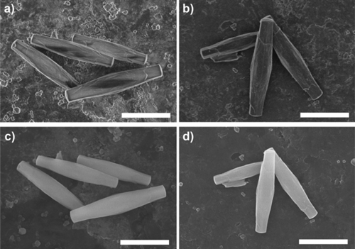 Figure 3. SEM images of PCN-222(Fe): with Os coating (a, c) and without coating (b, d), at 2 kV (a, b) and 15 kV (c, d). Scale bar: 5 μm.