You want lighting that adapts to every scenario. The top picks include the TELESIN C03 Phone Magnetic Beauty Fill Light, which features a rotatable design and magnetic base for easy placement. Many options offer 360° rotation, strong magnets, and rechargeable batteries, so you can brighten your workspace or living area without hassle. The table below shows one of the most popular choices in the Rotatable Circular Magnetic Light category.
Why Choose Rotatable Circular Magnetic Light?
Home Benefits
You want lighting that adapts to your daily needs. Rotatable Circular Magnetic Light options provide several advantages for your home.
-
You can save up to 90% on your energy bills compared to traditional lighting.
-
LEDs in these lights deliver high efficiency, often reaching up to 90%, while old incandescent bulbs fall below 10%.
-
You can install magnetic track lights quickly without special skills or tools.
-
You can easily reposition these lights, so you can change your lighting setup whenever you want.
-
Adjustable and positionable features let you tailor the light to your reading, relaxing, or working needs.
-
Dimmable options allow you to set the brightness for any activity or mood.
Tip: Place a Rotatable Circular Magnetic Light near your reading nook or kitchen counter for instant, focused illumination.
Work Advantages
You need reliable lighting for your workspace. Rotatable Circular Magnetic Light products offer practical solutions for work environments.
-
You can direct light exactly where you need it, thanks to 360° rotation and strong magnetic bases.
-
These lights help you see small details on your workbench, in your garage, or during repairs.
-
Quick installation means you spend less time setting up and more time working.
-
You can move the light as your project changes, so you always have the best visibility.
-
Dimmable and adjustable features let you control the intensity for delicate tasks or broad illumination.
Note: Many professionals choose these lights for their flexibility and energy savings, making them a smart investment for any workspace.
Rotatable Circular Magnetic Light models stand out for their adaptability. You can use them in many scenarios, from home improvement to automotive repair. The table below highlights their versatility:
|
Feature/Application |
Description |
|---|---|
|
360° Swivel Adjustability |
Position the light at any angle for optimal visibility in any environment. |
|
Automotive Maintenance and Repair |
Illuminate engine bays or undercarriages, reaching confined spaces easily. |
|
Home Appliance Servicing |
Retrieve screws or washers behind appliances without moving them. |
|
Workshop and Garage Organization |
Pick up small metal items from hard-to-reach places without dismantling. |
|
Electronic Device Repairs |
Retrieve tiny screws from devices without damaging components. |
You can rely on these lights for both everyday and specialized tasks. Their design ensures you always have the right lighting, wherever you need it.

Brightness & Light Quality
Lumens & Color Temperature
You want a light that delivers the right amount of illumination for your space. Lumens measure the total light output, so higher lumens mean a brighter environment. Most rotatable circular magnetic lights offer a wide range of brightness, with some models reaching up to 4541 lux at 1 meter. This level of output suits both detailed work and general room lighting.
Color temperature also plays a crucial role. You can select between warm white for a cozy atmosphere or cool white for a more focused, energetic workspace. Some advanced models feature RGBWW technology, allowing you to adjust the color spectrum for creative effects or mood lighting. The following table summarizes key brightness and color features you should consider:
|
Feature |
Details |
|---|---|
|
Lumens/Output |
Up to 4541 lux @ 1 m |
|
Color Options |
Warm white, cool white, RGBWW |
|
Beam Angle |
50° beam for focused or broad coverage |
Tip: Choose a light with adjustable color temperature if you want to switch between relaxing and working modes.
Dimmable Options
You need control over your lighting intensity. Dimmable options let you fine-tune brightness from 0% to 100%, often using a wheel or touchscreen interface. Stepless dimming ensures smooth transitions, so you avoid harsh changes in light. This feature proves essential for tasks that require precision, such as reading, crafting, or working on electronics.
Many lights include advanced controls, such as Bluetooth or Wi-Fi apps, enabling you to adjust settings remotely. Some models even offer cinematic effects like lightning or fire, which add versatility for photography or ambiance.
Rotation & Adjustability
You benefit from maximum flexibility when your light rotates freely. Most rotatable circular magnetic lights feature 360° adjustability, so you can direct illumination exactly where you need it. This capability allows you to reposition the light for different tasks, whether you are working under a car hood or highlighting a piece of art.
You can easily change the angle without detaching the light from its magnetic base. Some models include joysticks or touchscreens for precise control, making them suitable for both professional and home use.
-
360° rotation for full coverage
-
Quick angle adjustments for changing tasks
-
Joystick or touchscreen for fine-tuning
Magnetic Base Strength
You need a secure attachment for safety and convenience. The magnetic base determines how well the light stays in place on metal surfaces. Strong magnets prevent accidental falls and allow you to mount the light on vertical or overhead surfaces. You can reposition the light quickly, which is ideal for dynamic workspaces.
Some models offer additional mounting options, such as rear threads or cold-shoe adapters, expanding their versatility. Always check the magnet strength before purchasing, especially if you plan to use the light in demanding environments like garages or workshops.
Note: A robust magnetic base ensures your Rotatable Circular Magnetic Light remains stable, even during frequent adjustments.
Battery & Power
You need reliable power for your lighting. Battery life and type play a crucial role in how often you recharge or replace your light. Most rotatable circular magnetic lights use either standard alkaline batteries or rechargeable lithium-ion cells. The table below summarizes the average battery life for each type:
|
Battery Type |
Average Battery Life |
|---|---|
|
Standard Alkaline |
40-60 hours at full brightness |
|
Rechargeable Lithium-ion |
3-6 months with regular use |
You can choose a model based on your usage habits. If you want a light for occasional use, standard alkaline batteries may suffice. For frequent use, rechargeable lithium-ion batteries offer longer life and lower long-term costs. Many modern lights include USB-C charging, so you can recharge quickly and avoid downtime. Some models also feature battery level indicators, which help you plan ahead and avoid unexpected outages.
Tip: Always check the battery specifications before purchasing. A longer battery life means less maintenance and more consistent performance.
Mounting Options
You want flexibility in how you install your Rotatable Circular Magnetic Light. Different mounting options affect both the look and the ease of installation. The table below outlines the main choices:
|
Mounting Option |
Description |
|---|---|
|
Surface |
Easiest installation method, allows for flexibility and maintenance. |
|
Recessed |
Provides a seamless look but is more complex to install, requires careful alignment. |
|
Pendant |
Ideal for high ceilings, allows for visual impact and utility, requires precise drop length calculations. |
-
Surface-mounted tracks let you install and maintain your lights with minimal effort. You can reposition or add lights as your needs change.
-
Recessed systems create a clean, modern appearance. You need to plan carefully, especially if your ceiling has slopes or obstacles.
-
Pendant systems work well in rooms with high ceilings. They add style and function, but you must measure drop lengths accurately for the best effect.
Note: Consider your ceiling type and the intended use of the space before selecting a mounting option. The right choice ensures both safety and aesthetics.
Design & Durability
You expect your lighting to last and look good. Design and durability matter, especially in high-traffic or demanding environments. Many rotatable circular magnetic lights use aluminum or high-grade plastic for the housing. These materials resist scratches, dents, and corrosion. You can find models with water-resistant or dustproof ratings, making them suitable for garages, workshops, or kitchens.
Manufacturers often design these lights with smooth edges and compact profiles. This approach prevents snagging and allows for easy cleaning. Some models feature anti-glare lenses or frosted covers, which reduce eye strain and improve comfort. You should also look for lights with reinforced magnetic bases, as these withstand frequent repositioning without losing strength.
Pro Tip: Choose a light with a robust build and quality materials. A well-designed Rotatable Circular Magnetic Light will serve you reliably for years, even in tough conditions.

Top Rotatable Circular Magnetic Light Picks
You get a powerful lighting solution with the Husky 2200-Lumen Tripod K40437. This model delivers high brightness and wide coverage, making it suitable for demanding tasks. The tripod design gives you stability and height adjustment. You can rotate the light head to direct illumination exactly where you need it.
Pros & Cons
Pros:
-
High lumen output for large spaces
-
Adjustable tripod for flexible positioning
-
Durable construction for tough environments
-
Rotatable head for targeted lighting
Cons:
-
Bulkier than handheld models
-
Requires more storage space
-
Not as portable for quick tasks
Best Uses
You will find this light ideal for garage work, construction sites, and outdoor projects. It suits situations where you need strong, stable lighting over a wide area. You can also use it for home renovations or emergency repairs.
-
2200 lumens of bright, clear light
-
360° rotatable head for full coverage
-
Adjustable tripod height for custom setups
-
Rugged build for long-term use
KleverRoundLamp™
You experience a blend of style and function with the KleverRoundLamp™. This Rotatable Circular Magnetic Light offers smooth brightness adjustment and a 360-degree magnetic rotation. The lightweight design makes it easy to move from room to room. The wooden finish adds a touch of elegance to your decor.
Pros & Cons
Pros:
-
Lightweight and portable
-
Smooth dimming for precise control
-
Attractive wooden design
-
Strong adhesive for easy mounting
-
360-degree rotation for flexible lighting
Cons:
-
Adhesive may not suit all surfaces
-
Not designed for heavy-duty workspaces
Best Uses
You can use the KleverRoundLamp™ in bedrooms, living rooms, or study areas. It works well as a reading light, accent lamp, or night light. The design fits modern and minimalist interiors.
-
360-degree magnetic rotation for easy adjustment
-
Stepless brightness control for any mood
-
Strong adhesive backing—no drilling required
-
Elegant wood finish enhances any space
Customer feedback highlights the lamp’s portability, smooth dimming, and stylish design. Reviewers appreciate the 360-degree rotation and the convenience of adhesive mounting.
|
Reviewer |
Feedback |
|---|---|
|
S Satomi |
lightweight and easy to carry |
|
A Astrid |
smooth brightness adjustment |
|
H Haruto |
beautiful wooden design enhances decor |
|
O Oriana |
useful 360-degree magnetic rotation |
|
S Sofia |
strong adhesive saves hassle of drilling |
5000 Lumens LED Rechargeable Work Light
You get maximum brightness with the 5000 Lumens LED Rechargeable Work Light. This model suits users who need intense illumination for large or dark spaces. The rechargeable battery ensures you can work without worrying about cords. The magnetic base lets you attach the light to metal surfaces for hands-free operation.
Pros & Cons
Pros:
-
Extremely bright output for demanding tasks
-
Rechargeable battery for cordless use
-
Strong magnetic base for secure mounting
-
Rotatable design for flexible positioning
Cons:
-
May be too bright for small rooms
-
Heavier than compact models
-
Longer charging time for full battery
Best Uses
You will find this light perfect for workshops, garages, and outdoor repairs. It also works well for camping, emergency situations, and construction sites. The high lumen output covers large areas efficiently.
-
5000 lumens for superior brightness
-
Rechargeable lithium-ion battery for convenience
-
360° rotation for precise light direction
-
Durable housing for rugged environments
You can rely on this Rotatable Circular Magnetic Light for both professional and home use. The combination of brightness, battery power, and adjustability makes it a top choice for challenging tasks.
180 Lumen Rotating Magnetic LED Work Light
You get a compact and practical lighting solution with the 180 Lumen Rotating Magnetic LED Work Light. This model delivers reliable illumination for small tasks and tight spaces. The magnetic base allows you to attach the light to any metal surface, freeing your hands for work. The rotating head lets you direct the beam exactly where you need it, making it a versatile choice for both home and professional environments.
Pros & Cons
You can quickly assess the strengths and limitations of this work light by reviewing the table below:
|
Advantages |
Limitations |
|---|---|
|
Hands-free operation due to magnetic base |
Reliance on AAA batteries |
|
Ability to swivel light for precise direction |
Relatively short runtime of 3 to 6 hours |
|
Affordability |
|
Best Uses
You will find this light ideal for automotive repairs, electrical work, and DIY projects. It fits perfectly in toolboxes and glove compartments, so you always have a portable light source on hand. You can also use it for camping, emergency kits, or as a backup light during power outages.
Standout Features
-
180-lumen output for focused tasks
-
360° rotating head for precise light placement
-
Strong magnetic base for hands-free use
-
Lightweight and portable design
Tip: Keep a few of these lights in different locations around your home and workspace. You will always have quick access to reliable lighting when you need it most.
Adjustable Folding Magnetic Track Light 8W
You experience innovation and flexibility with the Adjustable Folding Magnetic Track Light 8W. This model stands out with its patented design and tool-free installation. The snap-fit magnetic system allows you to set up or reposition the light in seconds. You can customize the configuration to suit your lighting needs, making it a smart choice for modern interiors and dynamic workspaces.
Pros & Cons
You benefit from a unique combination of style, convenience, and safety. The light’s high-quality finish enhances any room, while its certifications ensure peace of mind. However, the advanced features may come at a higher price point compared to basic models.
Pros:
-
Patented and unique design
-
Tool-free, snap-fit magnetic installation
-
Multiple customization options
-
Excellent surface finish
-
Certified for safety and quality (CE / Rohs / ETL)
Cons:
-
Higher cost than standard models
-
May require compatible track system
Best Uses
You can use this light in living rooms, offices, galleries, or retail spaces. The folding and adjustable features make it perfect for highlighting artwork, illuminating workstations, or creating ambient lighting. You can easily adapt the setup as your needs change.
The following table highlights what sets this model apart:
|
Feature |
Description |
|---|---|
|
Patent and unique design |
Distinctive look and function not found in other lights |
|
Tool-free installation |
Snap-fit magnetic system for effortless setup |
|
Customization options |
Multiple configurations for personalized lighting |
|
Excellent surface finish |
Premium appearance for any setting |
|
CE / Rohs / ETL certified |
Meets international safety and quality standards |
Note: If you want a Rotatable Circular Magnetic Light that combines aesthetics, flexibility, and safety, this model delivers on all fronts.
Comparison Table
You want to make an informed decision when choosing a rotatable circular magnetic light. Comparing the top models side by side helps you see which features matter most for your needs. The table below highlights essential specifications, so you can quickly identify the best fit for your home or workspace.
|
Product Name |
Brightness (Lumens) |
Rotation Angle |
Battery Life |
Magnetic Strength |
Mounting Options |
Price Range |
|---|---|---|---|---|---|---|
|
Husky 2200-Lumen Tripod K40437 |
2200 |
360° |
Plug-in (no battery) |
Strong (tripod base) |
Tripod, surface |
$60 - $80 |
|
KleverRoundLamp™ |
Adjustable (up to 400) |
360° |
8-12 hours (rechargeable) |
Moderate (adhesive + magnet) |
Adhesive, magnetic |
$35 - $50 |
|
5000 Lumens LED Rechargeable Work Light |
5000 |
360° |
6-10 hours (rechargeable) |
Strong (heavy-duty magnet) |
Magnetic, portable |
$70 - $100 |
|
180 Lumen Rotating Magnetic LED Work Light |
180 |
360° |
3-6 hours (AAA batteries) |
Moderate (compact magnet) |
Magnetic, handheld |
$10 - $20 |
|
Adjustable Folding Magnetic Track Light 8W |
600 |
360° folding |
10-15 hours (rechargeable) |
Strong (track magnet) |
Track, surface |
$80 - $120 |
|
Square LED Work Light |
4200 |
170° bracket |
Plug-in (no battery) |
Strong (industrial magnet) |
Bracket, magnetic |
$50 - $75 |
Tip: If you need maximum brightness for large areas, choose the 5000 Lumens LED Rechargeable Work Light or the Square LED Work Light. For portable use and easy mounting, the KleverRoundLamp™ or the 180 Lumen Rotating Magnetic LED Light offer great flexibility.
How to Use the Table
-
Scan the brightness column to match your lighting needs. High lumen values suit garages and workshops. Lower values work well for reading nooks or accent lighting.
-
Check the rotation angle. Full 360° rotation gives you the most flexibility for directing light.
-
Review battery life. Rechargeable models save you money over time. Plug-in options provide unlimited runtime but less portability.
-
Assess magnetic strength. Strong magnets keep your light secure on metal surfaces. Moderate magnets work for lighter tasks.
-
Consider mounting options. Tripods and brackets offer stability. Adhesive and handheld designs provide quick setup.
-
Compare price ranges. Set your budget before you shop. Higher-priced models often include advanced features or certifications.
Note: You should always balance brightness, adjustability, and power source with your intended use. A light that excels in one area may not suit every situation.
Quick Checklist Before You Buy
-
Do you need portability or permanent installation?
-
Will you use the light for detailed work or general illumination?
-
Is battery life a priority for you?
-
Does your space have metal surfaces for magnetic mounting?
-
Are you looking for a specific design or finish?
You can use this comparison table to narrow down your choices. Select the model that matches your requirements and enjoy brighter, more flexible lighting in your home or workspace.
For Reading & Study
You need focused, comfortable lighting for reading and studying. Rotatable circular magnetic lights give you the flexibility to direct light exactly where you need it. Choose a model with adjustable brightness so you can set the perfect level for your eyes. Look for a light with a soft, warm color temperature. This reduces eye strain and helps you concentrate for longer periods. Many compact models offer 360° rotation, letting you position the beam over your book or workspace. You can attach these lights to metal shelves, desks, or even bed frames. Some designs include touch controls or stepless dimming, making it easy to adjust the light without interrupting your workflow.
Tip: Place your light above and slightly behind your reading area. This setup minimizes shadows and glare, creating a comfortable environment for study sessions.
For Workbench & Garage
You need a lighting solution that stands up to tough conditions in your workbench or garage. Select a rotatable circular magnetic light with a robust design. High-strength ABS material ensures the light can handle accidental drops and daily wear. A model offering 1500 lumens gives you enough brightness to see fine details during repairs or projects. You benefit from a head that rotates 180 degrees, allowing you to direct light into tight spaces or awkward angles. Three magnetic bases provide secure attachment to any metal surface, so your light stays in place even when you move tools or materials around. This combination of durability, brightness, and flexibility makes these lights ideal for demanding environments.
Note: A sturdy, bright work light with multiple magnetic bases helps you tackle complex tasks safely and efficiently.
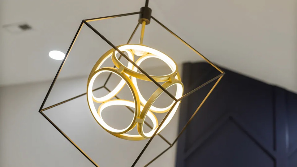
For Ambiance & Decor
You want lighting that enhances your space and sets the right mood. Rotatable circular magnetic lights designed for ambiance and decor offer features that blend style with function. These models focus on comfort, aesthetics, and adaptability. The tables below highlight the most important features to consider:
|
Feature |
Description |
|---|---|
|
Comfortable lighting without glare |
Ensures a pleasant atmosphere without harsh light |
|
Elegant body coating |
Enhances aesthetic appeal and decor integration |
|
External dimming interface |
Allows for customizable lighting intensity |
|
Feature |
Description |
|---|---|
|
Minimal glare |
Reduces eye strain and enhances comfort |
|
Adjustable cables |
Facilitates versatile installation in various spaces |
|
Professional atmosphere creation |
Provides precise control over lighting effects |
|
Feature |
Description |
|---|---|
|
Length adjustable cable |
Adapts to different room heights and layouts |
|
Comfortable lighting without glare |
Ensures a pleasant atmosphere without harsh light |
|
External dimming interface |
Allows for customizable lighting intensity |
You can use these lights to highlight artwork, create a cozy reading nook, or add a modern touch to your living room. Adjustable cables and dimming interfaces let you tailor the installation and brightness to match your decor and mood.
Pro Tip: Choose a model with minimal glare and an elegant finish to create a welcoming, stylish environment in any room.
For Portability & Emergency
You need lighting that adapts quickly when you face unexpected situations. Rotatable circular magnetic lights excel in portability and emergency scenarios. You can carry these lights anywhere because manufacturers design them with lightweight materials and compact shapes. You fit them in your backpack, glove compartment, or emergency kit without hassle.
You benefit from rechargeable batteries that deliver hours of illumination. Many models feature USB-C charging, so you power up with standard cables. You avoid searching for specialty chargers during critical moments. Some lights include battery level indicators. You check the charge status at a glance and prepare for outages or outdoor adventures.
You rely on strong magnetic bases to attach your light to metal surfaces. You work hands-free under the hood of your car or inside a dark closet. You rotate the light head to direct the beam exactly where you need it. This flexibility proves essential during repairs, roadside emergencies, or power failures.
Manufacturers often add weather-resistant features. You use these lights in rain, snow, or dusty environments. You trust the durable housing to protect the electronics. You avoid damage from drops or rough handling.
Consider the following table when selecting a portable or emergency light:
|
Feature |
Benefit |
|---|---|
|
Compact size |
Easy to carry and store |
|
Rechargeable battery |
Reliable power for extended use |
|
Magnetic base |
Hands-free operation on metal surfaces |
|
360° rotation |
Flexible beam direction |
|
Weather resistance |
Safe use in harsh conditions |
|
Battery indicator |
Quick status check for preparedness |
Tip: Keep one rotatable circular magnetic light in your car and another in your home emergency kit. You stay ready for blackouts, breakdowns, or outdoor activities.
You choose models with simple controls. You turn them on instantly with a single button. You adjust brightness for reading, signaling, or working. You avoid complicated settings that slow you down during emergencies.

Installation & Usage Tips
You want your rotatable circular magnetic light to stay secure and perform at its best. Start by choosing a clean, flat metal surface for mounting. Wipe away dust, oil, or moisture before you attach the magnetic base. This step ensures maximum grip and prevents accidental slips.
Position the light so you can easily reach the controls and adjust the angle. Avoid placing the light near strong electromagnetic sources, such as large motors or transformers. These can interfere with the magnetic hold.
If your model includes adhesive backing, press firmly for at least 30 seconds. Wait a few hours before you reposition the light. This waiting period allows the adhesive to bond fully. For track-mounted systems, align the connectors carefully and listen for a click to confirm a secure fit.
Tip: Test the stability by gently nudging the light after installation. If it moves easily, try a different spot or clean the surface again.
Mounting Checklist:
-
Clean the mounting surface
-
Check for metal compatibility
-
Avoid electromagnetic interference
-
Confirm secure attachment
-
Position for easy access
Battery Care
You rely on battery power for consistent lighting. To extend battery life, charge your light fully before first use. Use the recommended charger and avoid overcharging. Unplug the device once the battery indicator shows full capacity.
Store your light in a cool, dry place. Extreme heat or cold can damage battery cells and reduce performance. If you use alkaline batteries, replace them as soon as you notice dimming. For rechargeable models, cycle the battery every few months. This practice maintains optimal capacity.
Note: If you plan to store the light for a long period, remove the batteries. This step prevents leakage and corrosion.
|
Battery Type |
Care Tip |
Expected Lifespan |
|---|---|---|
|
Alkaline |
Replace when dim |
40-60 hours per set |
|
Lithium-ion (Rechargeable) |
Charge fully, avoid overcharging |
300-500 cycles |
Cleaning & Maintenance
You keep your light working longer with regular cleaning. Use a soft, dry cloth to wipe the housing and lens. Avoid harsh chemicals or abrasive pads. These can scratch the surface or damage the finish.
Inspect the magnetic base for dust or metal shavings. Clean with a gentle brush if needed. For track systems, check connectors for debris and clear them with compressed air.
If your light has a water-resistant rating, you can use a damp cloth for tougher stains. Dry the unit completely before reattaching it to any surface.
Pro Tip: Schedule monthly maintenance checks. Clean the lens, test the rotation, and inspect the battery compartment. This routine keeps your rotatable circular magnetic light in top condition.
Maintenance Steps:
-
Wipe surfaces with a soft cloth
-
Clean magnets and connectors
-
Check for loose parts or damage
-
Test rotation and adjustability
-
Replace or recharge batteries as needed
You ensure reliable performance and longer lifespan by following these simple care routines.
Safety Tips
You want your rotatable circular magnetic light to provide reliable illumination without risk. Following essential safety guidelines helps you avoid accidents and extends the life of your lighting investment. Use the following tips to ensure safe operation at home or work.
1. Prevent Overheating
Always monitor your light during extended use. LEDs generate less heat than traditional bulbs, but enclosed spaces can still trap warmth. Place your light in a well-ventilated area. Avoid covering the housing with fabric or paper. If you notice the light becoming hot to the touch, turn it off and let it cool before handling.
2. Avoid Water and Moisture
Most rotatable circular magnetic lights are not waterproof unless specifically rated. Keep your light away from sinks, bathtubs, and outdoor areas during rain. If you need to use your light in damp environments, check the IP (Ingress Protection) rating. Only use models with water-resistant certification for these situations.
Tip: If your light gets wet, disconnect it from power immediately. Dry it thoroughly before using it again.
3. Secure Mounting
You must ensure the magnetic base attaches firmly to a clean, flat metal surface. Test the stability by gently nudging the light. If it shifts or falls, reposition it or clean the surface again. Never hang heavy objects from the light or use it as a support. This prevents accidental drops and damage.
4. Battery Safety
Rechargeable models require proper battery care. Use only the charger provided by the manufacturer. Avoid overcharging or leaving the light plugged in for long periods. For models using disposable batteries, insert them in the correct orientation. Remove batteries if you plan to store the light for a long time.
|
Battery Type |
Safety Precautions |
|---|---|
|
Rechargeable |
Use original charger, avoid overcharging |
|
Disposable |
Insert correctly, remove for long storage |
5. Electrical Safety
If your light plugs into an outlet, inspect the cord and plug for damage before each use. Do not use the light if you see frayed wires or exposed metal. Keep cords away from walkways to prevent tripping hazards. Unplug the light before cleaning or moving it.
6. Child and Pet Safety
Keep lights out of reach of young children and pets. Small parts, magnets, and batteries can pose choking hazards. Teach children not to play with the light or its mounting system.
Note: Always follow the manufacturer’s instructions for installation and use. Proper handling ensures your safety and the longevity of your rotatable circular magnetic light.
By following these safety tips, you create a secure environment and maximize the performance of your lighting solution. You protect yourself, your family, and your workspace from unnecessary risks.
You have explored the best Rotatable Circular Magnetic Light options for home and work. Each pick offers unique strengths, from high brightness to flexible mounting. Focus on features like rotation, battery life, and magnetic strength when you choose. Use the comparison table and selection tips to guide your decision. Upgrade your lighting and create a brighter, more efficient environment today.