Latest Electronics News & Trends | Expert Insights & Innovations
FIB-SEM

CIQTEK DB550 FIB-SEM Prepares 5nm Chip Samples for TEM Analysis

CIQTEK DB550 Focused Ion Beam Scanning Electron Microscope

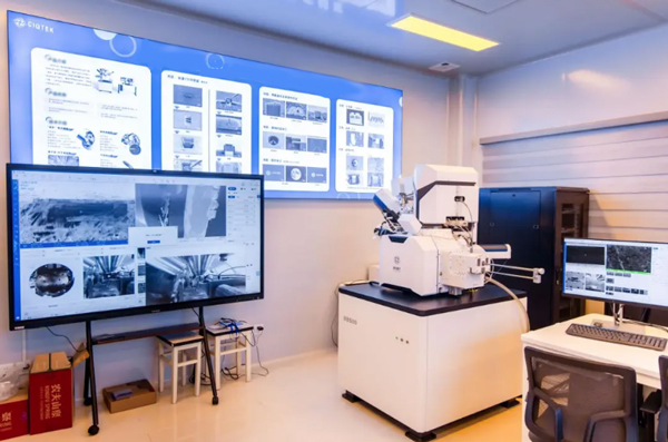
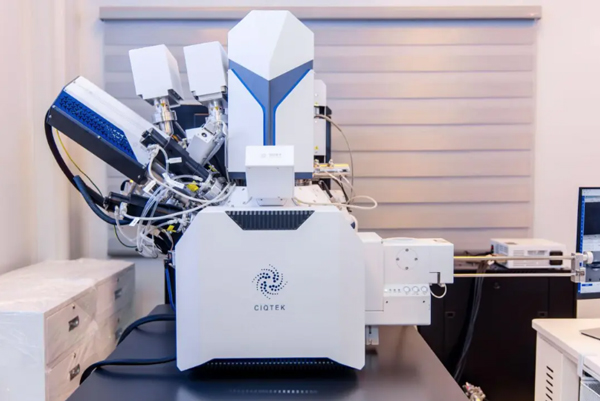
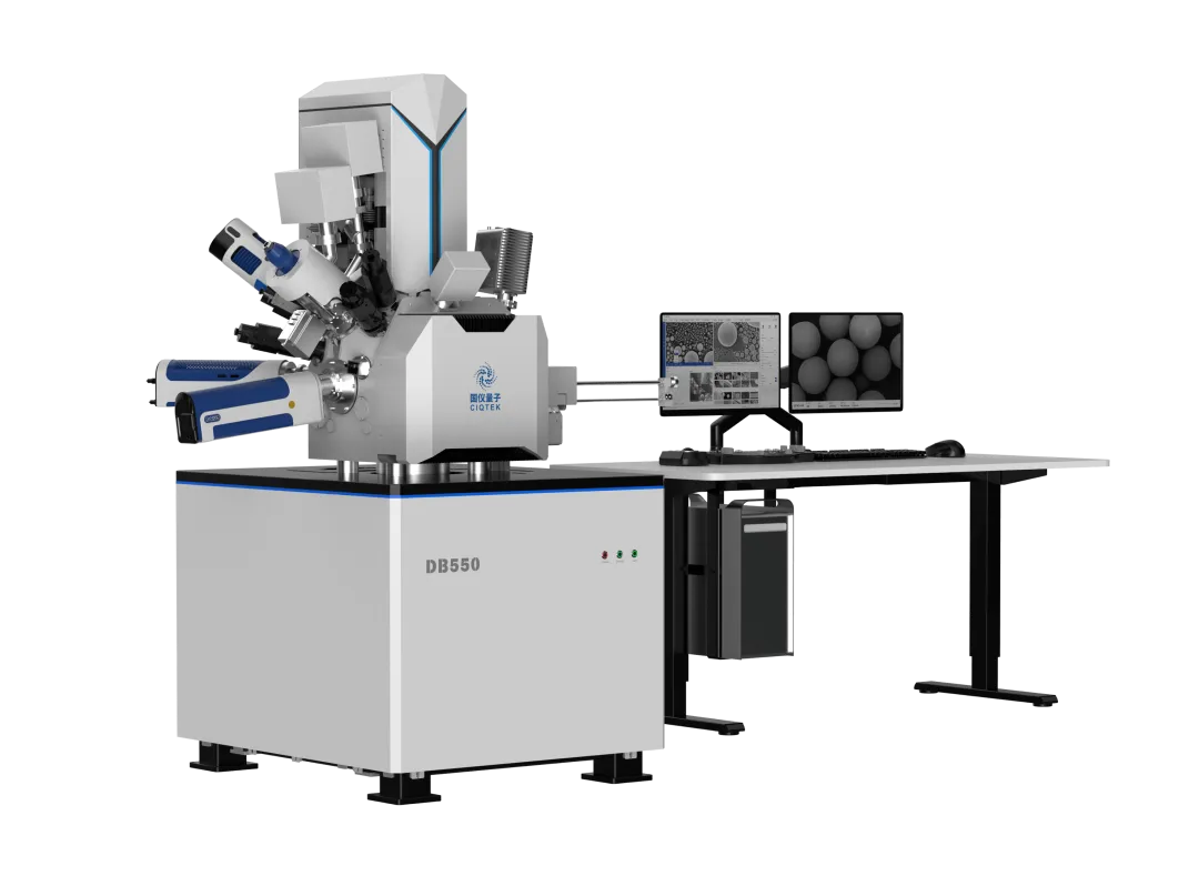
The CIQTEK DB550 dual-beam FIB-SEM brings together high-resolution electron imaging and precision ion beam processing on a single platform.

CIQTEK has validated its DB550 Focused Ion Beam Scanning Electron Microscope (FIB-SEM) on real 5nm process node chip samples, demonstrating production-ready TEM sample preparation with intact fin structures, zero amorphization, and clearly resolved film layers. The results confirm that the DB550 meets the exacting demands of advanced semiconductor failure analysis labs working at the cutting edge of process technology.

In advanced chip research and manufacturing, two tools matter above all others. The Transmission Electron Microscope (TEM) lets you see structures at the atomic scale. But before you can look, you need a sample thin enough for electrons to pass through. That is where the dual-beam FIB-SEM comes in. It is the precision workshop that prepares those ultra-thin specimens.

Meet the DB550: One Platform for Imaging and Nanoscale Processing

The CIQTEK DB550 FIB-SEM integrates two powerful capabilities onto a single platform. On one side, a scanning electron microscope (SEM) delivers high-resolution surface imaging. On the other, a focused ion beam (FIB) performs nanoscale material removal with surgical precision. Together, they bridge the gap between observation and fabrication at dimensions measured in billionths of a meter.

At the heart of the DB550 sits a low-voltage, high-resolution electron column paired with CIQTEK's proprietary "Chengying" ion column, developed entirely in-house. The Chengying column is the engine behind the system's nanoscale cutting and etching capabilities. CIQTEK controls the full design and manufacturing pipeline for this critical component.

The 5nm Challenge: Why Sample Preparation Gets Harder at Every Node

At 5nm and below, chip architectures rely on fin-type field-effect transistors (FinFETs) with fin widths and pitches measured in just a few nanometers. The DB550 is designed to handle the full sample preparation workflow for these demanding process nodes. It starts with high-current rough cutting to quickly remove bulk material and reach the target region. Then it transitions to low-voltage fine polishing to thin the sample to TEM-ready dimensions without damaging the delicate structures underneath.

TEM Validation: The Proof Is in the Image

CIQTEK prepared a 5nm process node chip sample on the DB550 and transferred it to a TEM for characterization. The results speak for themselves.

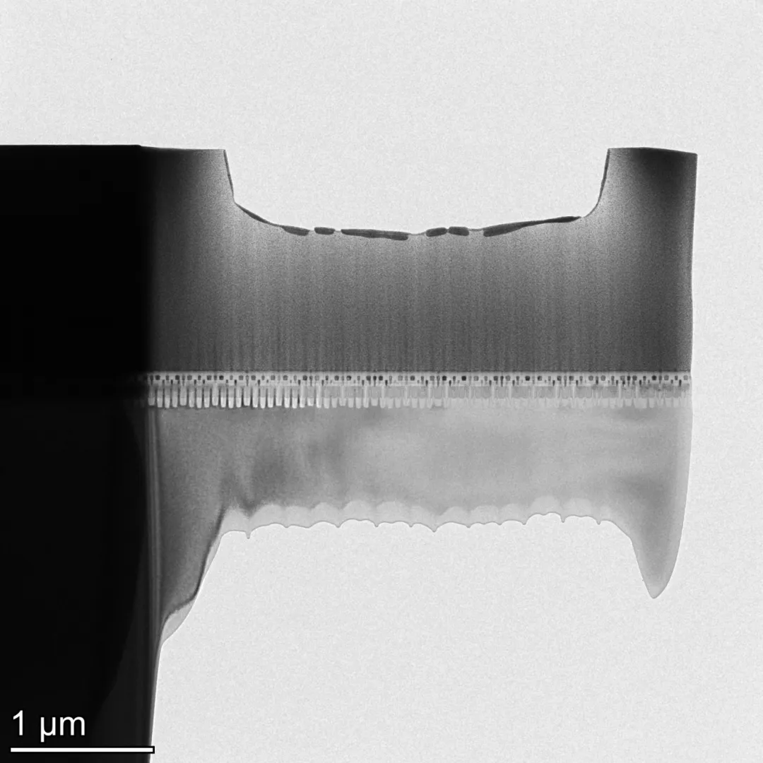
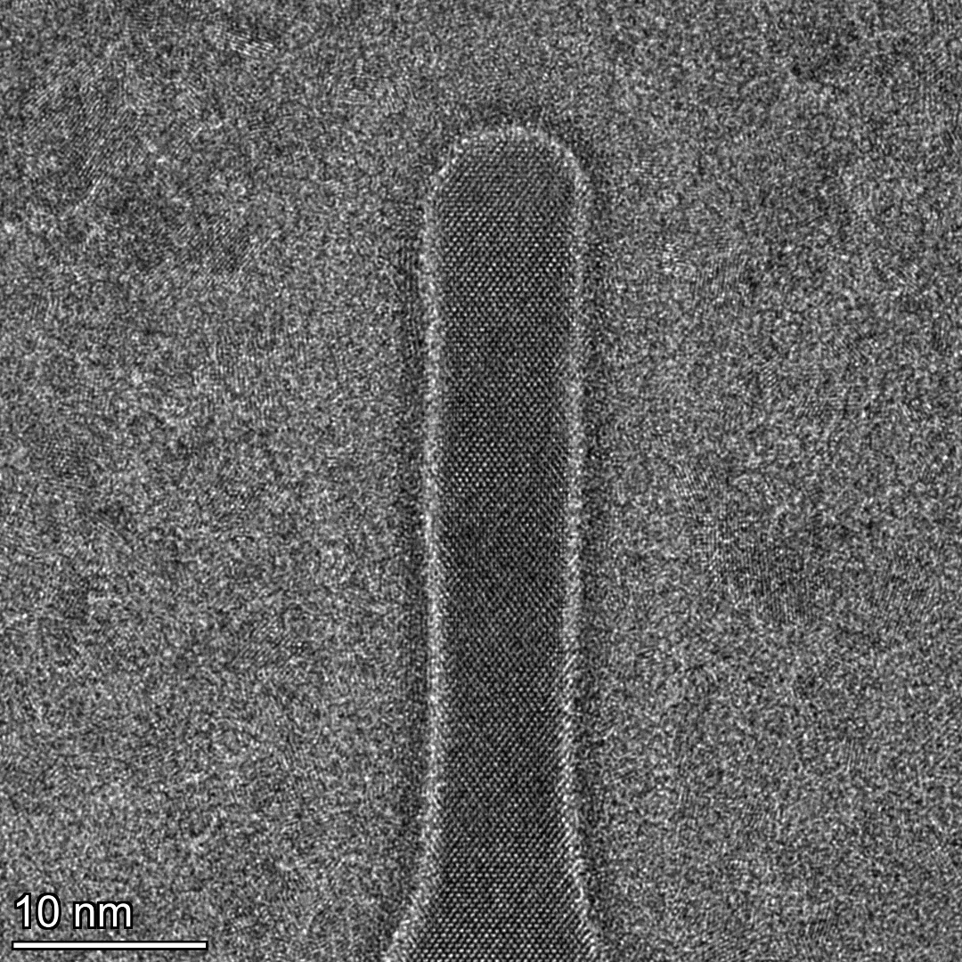
TEM characterization of a 5nm chip sample prepared on the DB550 shows intact fin structures with clear, well-defined film layers and no amorphization damage.

The TEM images revealed that the fin structures remained completely intact after FIB preparation. There was no detectable amorphization in the silicon crystal lattice. The individual film layers appeared clear and sharply defined in the TEM cross-section. These results validate the dual-beam sample preparation performance of the DB550 on the most advanced process nodes.

Engineered for Reliability, Built for the Long Term

Electron microscopes are the core tool in semiconductor failure analysis labs. CIQTEK develops the DB550 from the ground up, covering the full technology stack from core hardware to underlying algorithms. The proprietary Chengying ion column, the electron optics, the stage mechanics, and the control software are all designed and optimized as an integrated system.

Owning the full design strengthens supply chain resilience. Every critical component is sourced through CIQTEK's controlled development pipeline. For semiconductor labs that depend on instrument uptime for production yield analysis and failure investigations, this predictability matters.

CIQTEK backs the DB550 with continuous, reliable, and responsive technical support. The company also provides application support to help labs develop and optimize preparation recipes for new process nodes and novel device architectures.

阅读全文......

CIQTEK and USTC Mark One Year of Collaboration at the High-End In Situ Electron Microscopy Joint Laboratory

Advanced instruments alone do not drive scientific breakthroughs. Real progress happens when technology and researchers work closely together.


One year after the launch of the High-End In Situ Electron Microscopy Joint Laboratory, the collaboration between the Engineering and Materials Science Experimental Center and CIQTEK has shown how a shared innovation mindset can unlock new possibilities in in situ materials research, micro- and nano-fabrication, and mechanics-related studies.

"Choosing CIQTEK was never just about purchasing an instrument," says Professor Ming Gong, Deputy Director of the Engineering and Materials Science Experimental Center."We chose a partner who could work with us to explore and solve frontier scientific challenges."


A Core Research Platform Powered by In Situ Electron Microscopy

The Engineering and Materials Science Experimental Center is one of six university-level public experimental platforms at the University of Science and Technology of China. It supports a wide range of disciplines, including mechanics, mechanical engineering, instrumentation science, and engineering thermophysics.

The center plays a key role in advancing research on material mechanical behavior, complex fluid systems, precision measurement, micro- and nano-device fabrication, and renewable energy materials. By combining open access with professional analytical services, it enables interdisciplinary collaboration and connects academic research with real industrial needs.

Within this framework, in situ electron microscopy has become a critical capability. It allows researchers to directly observe structural and functional changes in materials under real conditions, providing insights that traditional post-analysis methods cannot deliver.


Why a FIB-SEM Dual-Beam Microscope Matters

As materials science research continues to move toward smaller length scales and more dynamic processes, traditional sample preparation methods are no longer sufficient. Modern studies increasingly require site-specific preparation, in situ observation, and three-dimensional reconstruction at the micro- and nano-scale.

To meet these demands, the center introduced a FIB-SEM dual-beam electron microscope, supplied by CIQTEK. This advanced scientific instrumentation enables precise micro- and nano-fabrication while maintaining high-resolution imaging performance, making it an essential tool for frontier research.

"Our goal was very clear," Professor Gong explains. "We wanted to provide advanced experimental conditions that support breakthroughs in frontier science and engineering, while also offering a strong technical foundation for future industrial innovation."


CIQTEK FIBSEM at the High-End In Situ Electron Microscopy Joint LaboratoryCIQTEK FIBSEM at the High-End In Situ Electron Microscopy Joint Laboratory


Choosing CIQTEK: Technology, Reliability, and Collaboration

During the instrument selection process, the center focused on three core factors: system stability, performance precision, and long-term technical support.

"The core specifications of CIQTEK's FIB-SEM are already on par with world-leading systems," says Professor Gong. "That gave us confidence from the start. What truly convinced us, however, was CIQTEK's openness to collaboration."

CIQTEK worked closely with researchers to understand real experimental needs, offering flexible support in application development and software compatibility. This approach turned the dual-beam electron microscope into a platform that could continuously evolve with ongoing research rather than remain a fixed configuration.


More Than Equipment: A Long-Term Research Partner

After more than a year of daily operation, the CIQTEK FIB-SEM dual-beam electron microscope has proven to be stable and reliable under high-intensity research conditions.

"The overall experience has exceeded our expectations," says Yu Bai, engineer at the Engineering and Materials Science Experimental Center. "The system performs consistently well in both micro- and nano-fabrication and high-resolution imaging, which is essential for our in situ materials research."

Just as important, CIQTEK has continued to track user feedback and translate research challenges into concrete optimization and upgrade directions. This ongoing interaction ensures that the instrument remains aligned with evolving experimental needs.


Fast Response to Non-Standard Experimental Challenges

One example clearly illustrates the value of this collaboration. During a project that went beyond the standard application scenarios of the system, the research team encountered a critical technical bottleneck.

"CIQTEK's application engineers came on site immediately," Bai recalls. "They worked with us to refine the experimental approach and quickly delivered a customized software upgrade."

This rapid response allowed the team to complete the experiment successfully and demonstrated how university–industry collaboration can directly accelerate scientific progress.

"At that moment, we truly felt what it means to have a partner," Bai adds. "Not just an equipment supplier, but a team that stays with us throughout the innovation process."


CIQTEK FIBSEM


Looking Ahead: Advancing In Situ Materials Research Together

The collaboration between the Engineering and Materials Science Experimental Center and CIQTEK offers a clear example of how advanced scientific instrumentation and close cooperation can support independent innovation.


As the High-End In Situ Electron Microscopy Joint Laboratory continues to develop, both sides will further focus on in situ materials research related to mechanics, micro- and nano-fabrication, and advanced experimental methodologies. Through continued collaboration, they aim to provide strong technical support for high-level research and future scientific breakthroughs.

阅读全文......