CIQTEK U.S. Team: Localized Expertise and Support
Strategic Significance: Academic Engagement and Regional Growth
Focus on Scanning Electron Microscopy (SEM) Technology
阅读全文......
CIQTEK participated in the TMS 2026 Annual Meeting & Exhibition, held from March 15–19, 2026 in San Diego, California, USA. Our U.S. team and local distribution partner welcomed visitors at Booth #307, where we presented our latest electron microscopy solutions for materials science applications.
Organized by The Minerals, Metals & Materials Society (TMS), this annual meeting is a key event for the global materials science community. It brings together researchers, engineers, and industry professionals working in areas such as metallurgy, advanced materials, additive manufacturing, and characterization technologies.
The event provides a strong platform for exchanging ideas, discovering new technologies, and discussing real-world challenges in materials research and production.
CIQTEK showcased electron microscopy solutions designed to support a wide range of materials science applications.
Our systems are well-suited for:
Microstructure analysis of metals and alloys
Failure analysis and defect investigation
Powder and particle characterization
Additive manufacturing and new materials research
Many visitors were particularly interested in how CIQTEK systems deliver stable imaging performance while remaining easy to operate. For labs balancing performance, usability, and budget, this combination is especially important.
We also had in-depth discussions with users about their daily challenges, such as improving imaging efficiency, simplifying workflows, and handling complex samples. These conversations help us better align our solutions with real application needs.
Participation in TMS 2026 is part of CIQTEK's broader strategy to expand its electron microscopy business in the U.S. market.
We offer:
A U.S.-based demo center for hands-on evaluation
U.S. Local technical and application support
Faster response for service and training
We continue to invest in local teams, infrastructure, and partnerships to support researchers and industry users better. By combining competitive technology with localized service, CIQTEK aims to make high-quality electron microscopy more accessible across North America.
Contact our U.S. team directly: info.usa@ciqtek.com
CIQTEK recently wrapped up an intensive two-day training program at the University of Science and Technology of China (USTC). By combining deep-dive theory with hands-on practice, our team helped nearly 60 researchers move beyond just "using" electron microscopes to truly mastering them for advanced semiconductor research.
At CIQTEK, we believe that high-end scientific instruments are only as powerful as the hands that operate them. Recently, our Customer Success team visited the Integrated Circuit Experiment Center at USTC. Our mission was simple: to take the complexity out of Scanning Electron Microscopy (SEM) and provide researchers with the practical skills they need to push the boundaries of micro-scale observation.
This "Service-First" initiative brought together about 60 students and faculty members for a deep dive into the world of precision microscopy.
A great experiment starts with a solid understanding of the "why" behind the "how." The training was structured into a dual-track model: comprehensive theory followed by intensive group practice.
In the classroom, our Customer Success Manager, Zhang Jing, broke down complex concepts into easy-to-digest insights. The sessions covered everything from the basic physics of electron beams to advanced parameter optimization.
Specifically, we focused on:
The Fundamentals: How SEM works and its core functional applications.
Optimization: Tweaking key parameters to get the sharpest possible data.
Semiconductor Focus: Specific characterization techniques tailored for integrated circuit research.
By simplifying the "hardcore" technical knowledge, we ensured every participant had a rock-solid foundation before they ever touched the equipment.

The real magic happened during the practical sessions. We know that reading a manual is never the same as actually running a scan. That is why our team moved into the lab for "shoulder-to-shoulder" teaching.
During the small-group workshops, we guided participants through the entire workflow:
Sample Preparation: The crucial first step for any successful scan.
Machine Operation: Getting comfortable with the CIQTEK hardware interface.
Image Analysis: Learning how to interpret what you are seeing.
Troubleshooting: Identifying and fixing common issues on the fly.
This one-on-one approach meant we could correct mistakes in real-time and answer specific questions as they popped up. The result? A noticeable jump in operating efficiency and a lot of happy researchers who now feel confident working with our instruments.


CIQTEK’s roots are in the academic world, and we feel a deep responsibility to give back to the scientific community. Our philosophy is built on "Achieving Customer Success." For us, the relationship does not end when an instrument is delivered; that is just where it begins.
We provide a full-spectrum service to protect your research journey:
Smooth Delivery: Getting your equipment set up and ready to run.
Deep Training: Ensuring your team has the skills to get the best results.
Daily Maintenance: Keeping the hardware in peak condition.
Ongoing Technical Support: We are just a call or email away when you hit a roadblock.
By providing this end-to-end support, CIQTEK is proud to safeguard the innovations happening in university labs and support the next generation of semiconductor and integrated circuit research.

While this two-day session has come to an end, our journey with the research community never stops. CIQTEK will continue to listen to user needs and provide the professional, attentive service that scientists deserve. We want our electron microscopes to be more than just tools; we want them to be reliable partners on your path to discovery.
Whether you are exploring the micro-world or breaking the boundaries of materials science, we are right there with you.
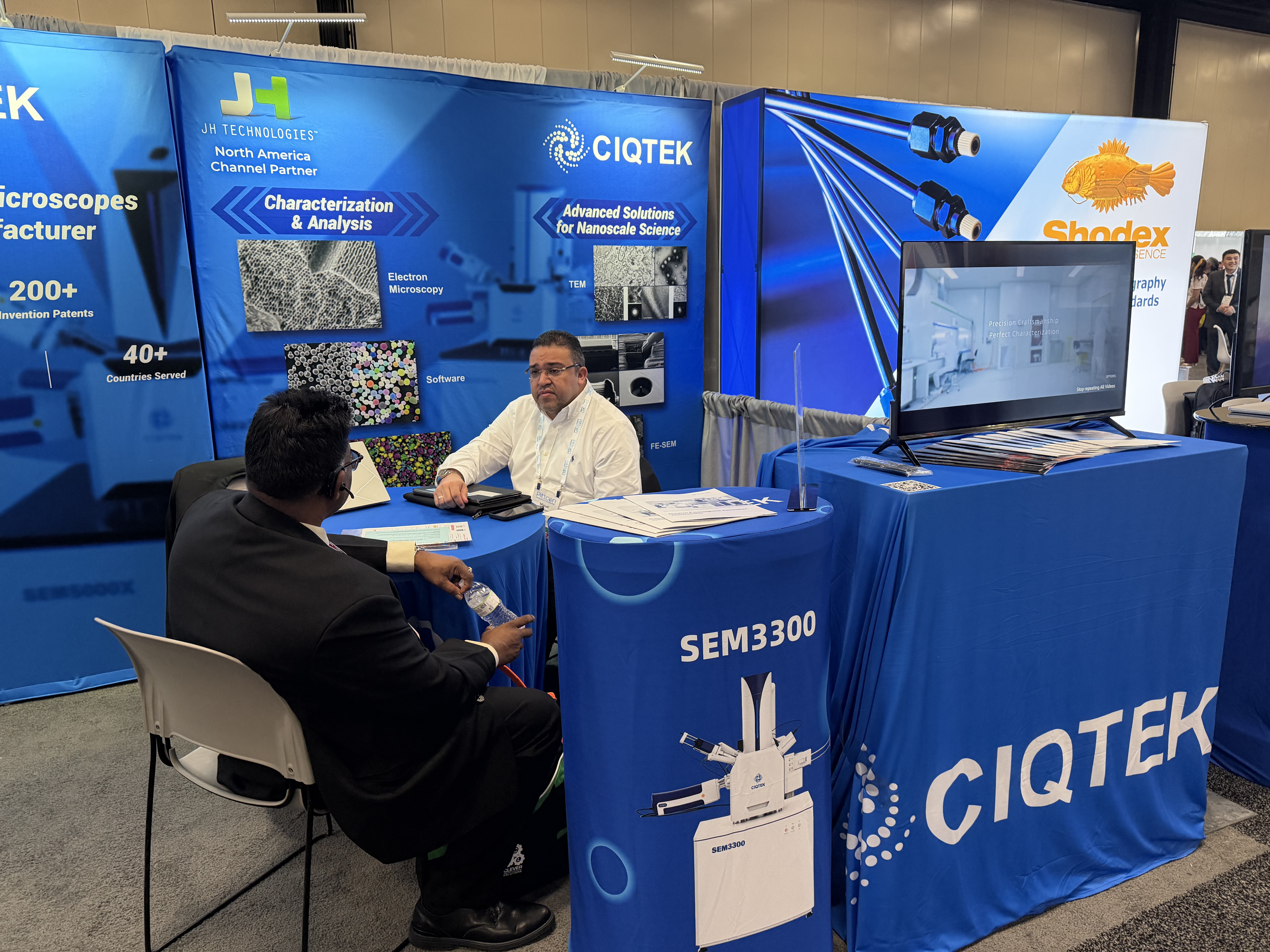
CIQTEK successfully participated in Pittcon 2026, March 9–11, San Antonio, TX, connecting with researchers, instrument specialists, and industry professionals from across North America and around the world.
At booth #1113, the CIQTEK team presented its latest solutions in electron microscopy, NMR and EPR spectroscopy, and gas adsorption analysis, drawing strong interest from visitors working in materials science, chemistry, and advanced research.
Supported by the CIQTEK U.S. team and local distribution partners, the booth provided a welcoming space for in-depth technical discussions and live demonstrations. Many visitors stopped by to learn more about CIQTEK instruments and explore how these technologies can support their research projects.
Electron microscopy was one of the key highlights at the CIQTEK booth. Visitors had the opportunity to learn about CIQTEK electron microscopy (SEM/FIB, TEM) solutions, designed to provide reliable high-resolution imaging for a wide range of applications.
Researchers from universities and research laboratories were particularly interested in how CIQTEK SEM systems can support materials characterization, nanostructure analysis, and semiconductor research. The CIQTEK team shared real application examples and discussed how stable imaging performance and user-friendly operation can help laboratories obtain high-quality results more efficiently.
CIQTEK also introduced its portfolio of Nuclear Magnetic Resonance (NMR) and Electron Paramagnetic Resonance (EPR) spectrometers, which attracted strong interest from scientists in chemistry, catalysis, and materials research.
Many visitors were interested in CIQTEK benchtop EPR solutions, designed to make EPR spectroscopy more accessible to laboratories seeking compact systems with strong performance. Discussions at the booth covered a range of applications, including studies of free radicals, transition metal ions, and material defects.
In addition to electron microscopy and EPR, CIQTEK presented its gas adsorption analyzers for surface area and pore structure characterization. These instruments are widely used in research areas such as catalysts, energy materials, porous materials, and environmental science.
Visitors were interested in discussing measurement workflows, data interpretation, and how gas adsorption techniques can complement other characterization methods in materials research.
With support from the CIQTEK U.S. team and local partners, CIQTEK continues to expand its presence in the North American market and provide responsive technical support to customers!
Contact our USA team: info.usa@ciqtek.com
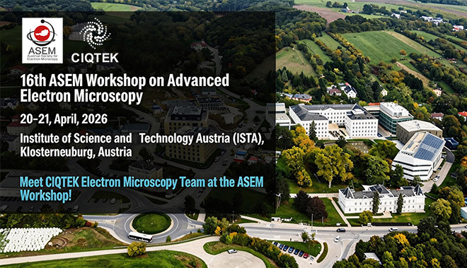
CIQTEK will attend the 16th Austrian Society for Electron Microscopy (ASEM) Workshop on Advanced Electron Microscopy, taking place on April 20–21, 2026, at the Institute of Science and Technology Austria (ISTA) in Klosterneuburg, Austria.
The workshop brings together researchers, engineers, and microscopy experts to explore the latest advancements in electron microscopy technologies, SEM imaging, and scientific applications.
At the event, the CIQTEK Electron Microscopy EU team will introduce its scanning electron microscopy (SEM) and field emission SEM (FE-SEM) systems, highlighting applications in materials science, nanotechnology, semiconductor research, and life sciences. Participants can learn about CIQTEK's high-performance, reliable, and user-friendly electron microscopes designed to meet diverse research needs.
In addition, Dr. Fengfa Yao, senior EM solution scientist from the CIQTEK EU Electron Microscopy team, will deliver a technical presentation titled "Unlocking the Power of Unique High-Speed Scanning Electron Microscopy with No Compromise of Superb Imaging Resolution at Low kV for Large Scale Volume Microscopy Applications from CIQTEK." The talk will introduce CIQTEK's latest advancements in high-speed SEM imaging, demonstrating how researchers can achieve rapid data acquisition while maintaining excellent low-kV imaging resolution, which is critical for large-scale volume microscopy applications.
To better serve European clients, CIQTEK has established and is expanding its dedicated DACH region (Germany, Austria, Switzerland) Electron Microscopy team, providing localized sales, technical support, and service. This ensures rapid response and tailored solutions for research institutes and laboratories across the region.
Event: 16th ASEM Workshop on Advanced Electron Microscopy
Date: April 20–21, 2026
Location: Institute of Science and Technology Austria (ISTA), Klosterneuburg, Austria
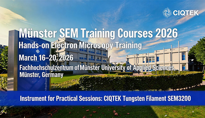
CIQTEK is pleased to announce that the CIQTEK SEM3200 tungsten filament scanning electron microscope will take part in the 2026 Münster SEM training courses, providing hands-on instrument experience for participants during the sessions held from March 16 to March 20, 2026 in Münster, Germany.
This collaboration allows researchers, engineers, and microscopy users attending the training program to directly operate the SEM3200 system and explore its capabilities in real-world analytical workflows. For many participants, it will be an opportunity to gain practical experience with modern scanning electron microscope technology during one of Europe’s longest-running microscopy training programs.
The SEM training courses in Münster are organized by the Akademie für Elektronenmikroskopie und Analytik gGmbH, a well-established institution dedicated to education in electron microscopy and microanalysis.
For decades, the academy has hosted intensive training sessions covering topics such as:
Scanning Electron Microscopy Fundamentals
Energy Dispersive Spectroscopy (EDS) analysis
Electron imaging techniques
Sample preparation and practical workflows
Data interpretation for materials analysis
These courses attract a diverse group of participants each year. Attendees include university researchers, laboratory engineers, industrial materials specialists, and microscopy facility staff from across Europe and beyond.
The training takes place at the Fachhochschulzentrum of Münster University of Applied Sciences, where lecture sessions are combined with hands-on laboratory work. Multiple microscopes are installed for the courses so that participants can gain direct operational experience.
The 2026 course schedule includes several specialized sessions, such as:
R-1: Introduction to Scanning Electron Microscopy
R-2: Advanced SEM and Microanalysis
R-3: Advanced SEM Techniques
EBSD Analysis Training
Particle Analysis Courses
During the sessions from March 16 to March 20, the CIQTEK SEM3200 will be available as one of the instruments used for training and demonstrations.
Check the courses here: http://www.akademie-elektronenmikroskopie.de/uebersicht.php
Training programs like the Münster SEM courses play an important role in the electron microscopy community. They provide a platform where researchers and engineers can strengthen their practical skills and exchange experiences with instructors and fellow participants.
CIQTEK believes that hands-on education is essential for advancing scientific research and analytical capabilities. By supporting training initiatives and providing instruments for practical sessions, the company aims to help users gain a deeper familiarity with SEM technology and its applications.
Events like these also create opportunities for dialogue between instrument developers and end users. Feedback from training environments often helps drive improvements in usability, software design, and analytical workflows.
The SEM3200 is part of CIQTEK's growing portfolio of electron microscopy instruments designed for research laboratories, universities, and industrial analytical facilities.
CIQTEK offers a range of scanning electron microscope solutions, including:
Reliable and cost-effective systems for routine imaging and materials analysis.
High-resolution instruments designed for advanced nanostructure observation and demanding research applications.
Dual-beam systems for nanoscale sample preparation, cross-sectioning, and 3D analysis.
The 2026 Münster SEM training courses will once again bring together members of the microscopy community for several weeks of intensive learning and practical experience. CIQTEK is pleased that the SEM3200 scanning electron microscope will contribute to the program and support participants during their hands-on sessions.
By working with training institutions and research organizations, CIQTEK continues to support the development of microscopy expertise and the advancement of materials characterization technologies worldwide.
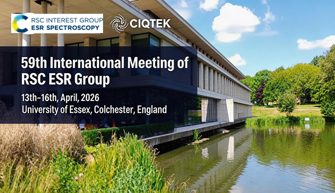
CIQTEK will exhibit at the 59th International Meeting of the RSC ESR Group together with our UK partner SciMed. We will display the CIQTEK EPR200M benchtop EPR spectrometer on site, fully installed and ready for live demonstration and sample testing.
The event will take place from April 13th to 16th at the University of Essex in Colchester, England. If you are working in EPR spectroscopy UK, this is a great chance to see our system up close and try it yourself.
At this year's meeting, we will also bring the real instrument as always!
The CIQTEK EPR200M is our compact X-band benchtop EPR system designed for:
University teaching labs
Routine research measurements
Industrial quality control
Entry-level EPR users
Labs looking for a cost-effective second system
During the conference, visitors will be able to:
See the EPR200M operating in real time
Explore the software interface
Discuss system configuration in detail
Bring samples for on-site testing
Talk directly with CIQTEK engineers and SciMed specialists
We know that for many researchers, performance claims only matter when you see real data. That is why we encourage you to bring your own samples. There is no better way to evaluate an EPR spectrometer than by running your own experiment.
While the EPR200M will be physically displayed, CIQTEK offers a full portfolio of EPR spectrometer systems to meet different research levels and application needs.
Designed for high sensitivity and stable long-term operation. Suitable for routine measurements and advanced research applications across chemistry, materials science, and life sciences.
Built for users working in spin dynamics, quantum materials, and biological structure studies. These systems provide precise microwave pulse control and flexible expansion for advanced experiments.
Compact and accessible systems such as the EPR200M, ideal for teaching labs, routine analysis, and industrial use.
In addition to new instruments, CIQTEK provides upgrade solutions for aging EPR systems. Many laboratories have legacy EPR spectrometers with stable magnets but outdated electronics or control systems. Our upgrade solutions can:
Modernize microwave bridges and control units
Improve signal-to-noise performance
Update software interfaces
Extend instrument service life
Reduce the need for full system replacement
For labs with budget constraints or long-term infrastructure considerations, upgrading can be a smart and practical path forward. We will be happy to discuss specific upgrade scenarios during the meeting.
The RSC ESR Group meeting is one of the key annual gatherings for the UK Electron Paramagnetic Resonance community. It brings together scientists from chemistry, physics, materials science, life sciences, and industry.
Over four days, participants share research results, discuss technical challenges, and explore new instrumentation solutions. The atmosphere is focused and highly interactive, which makes it ideal for in-depth technical conversations.
We are proud to support this community and to participate alongside our UK distributor.
CIQTEK will exhibit together with SciMed, our official partner in the United Kingdom.
Through this partnership, UK users benefit from:
Local sales and application consultation
Installation and training support
Responsive service and maintenance
Long-term upgrade planning
When investing in an Electron Paramagnetic Resonance system, support and reliability are just as important as specifications. With SciMed’s local presence and CIQTEK's engineering team, UK customers have both.
Event: 59th International Meeting of the RSC ESR Group
Date: April 13th to 16th, 2026
Location: University of Essex, Colchester, England
If you are attending the meeting, please stop by our booth to see the CIQTEK EPR200M live. You are also welcome to contact us in advance to schedule a dedicated discussion or sample testing time.
We look forward to meeting the UK EPR community in person and showing how the CIQTEK EPR spectrometer portfolio can support your research and applications.
2026 is a fresh start for CIQTEK Electron Microscope USA operations.
This year, we officially formed a dedicated CIQTEK US team. That means more local presence, faster response, and closer communication with customers across the country.
And we are not staying behind a desk.
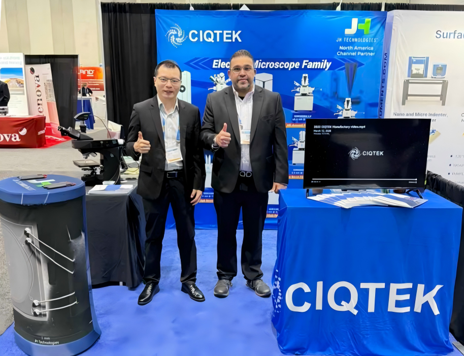
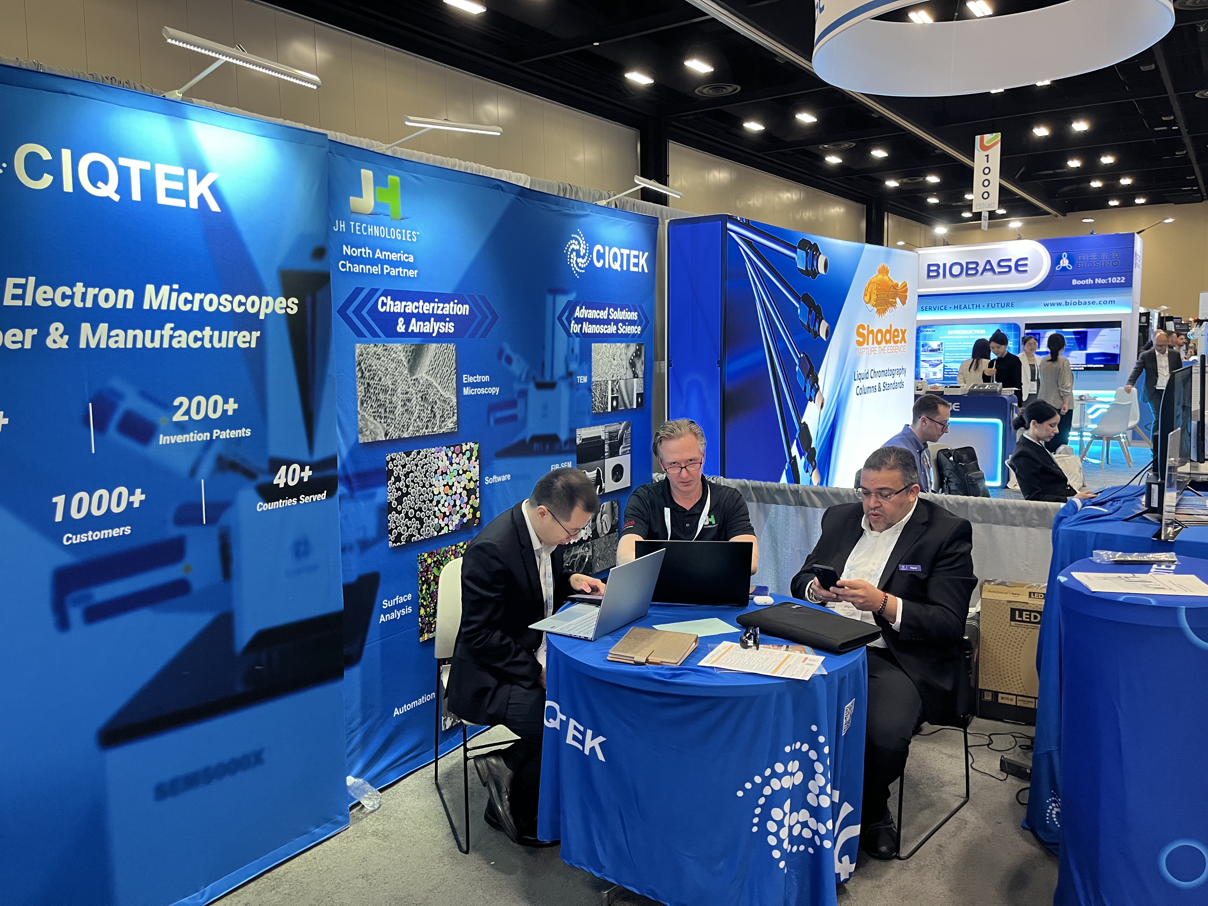
Our U.S. team, together with our official local distributor, JH Technologies, recently participated in the SMTA Wafer-Level Packaging Symposium 2026 and the 60th Anniversary Meeting of the Texas Society for Microscopy (TSM).
At the SMTA Wafer-Level Packaging Symposium in San Francisco, we connected with engineers and technical experts working in advanced semiconductor packaging.
As devices continue to shrink, inspection and defect analysis become more demanding. Reliable SEM solutions USA customers can trust are more important than ever. We had open, practical conversations about real challenges in wafer-level packaging. Topics included imaging resolution, surface characterization, and process optimization.
These discussions help us better understand how the CIQTEK electron microscope can support advanced manufacturing and research applications.
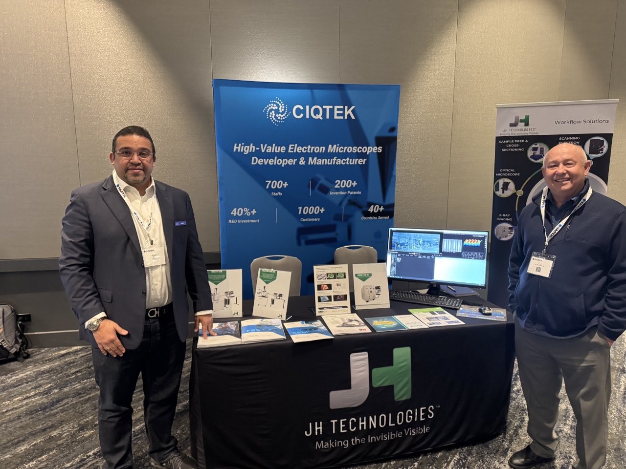 CIQTEK and JH Technologies at the SMTA 2026
The 60th Anniversary Meeting of the Texas Society for Microscopy was especially meaningful.
Unlike large national exhibitions, microscopy society events in the USA, such as TSM, allow for closer, more personal conversations. We met researchers, lab managers, and industry professionals from materials science, life sciences, and industrial labs.
For CIQTEK, TSM 2026 is the starting point of a broader plan. Our new CIQTEK US team will continue visiting regional microscopy societies across the country. We believe real relationships are built face-to-face.
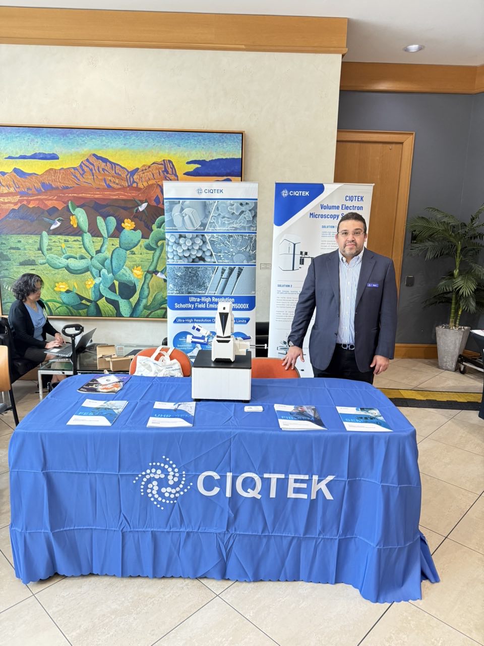 CIQTEK at the TSM 2026
The launch of our CIQTEK US team marks a new phase for CIQTEK electron microscope USA development.
We are investing in local support.
We are building stronger partnerships.
We are becoming part of the American microscopy ecosystem.
More regional visits are coming.
More technical exchanges are ahead.
2026 is not just another year. It is the year CIQTEK steps closer to the U.S. microscopy community.
And this is only the beginning.
The energy was intense. The snow was flying. The crowd was electric.
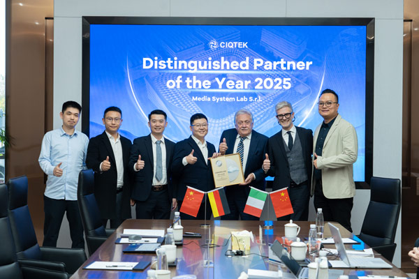
As part of our Winter Olympics 2026 story, CIQTEK invited our Italian partner Media System Lab to attend the competition at Livigno Snow Park as our special on-site representative.
They were there in person. Right at the venue. Capturing the atmosphere, the emotion, and the unforgettable moments from the 2026 Winter Olympics.
It was powerful. And it reminded us why the Olympic spirit matters far beyond sports.
At CIQTEK, we develop advanced scientific instruments, including SEM, NMR, EPR, BET systems, etc. Our work supports researchers who spend years chasing answers that most people never see.
Scientific progress is not instant. It takes patience. It takes resilience. It takes the willingness to refine and improve again and again.
That is why the scientific spirit aligns so naturally with the Olympic spirit.
Both are about:
Relentless improvement
Long-term commitment
Precision and control
Teamwork across borders
At Livigno Snow Park, our partner Media System Lab witnessed elite athletes pushing their physical limits. Back in laboratories around the world, scientists push technological and intellectual limits every day.
Different fields. Same mindset.
Global innovation depends on trusted partnerships. CIQTEK's collaboration with Media System Lab reflects our belief that strong local partners create a stronger global impact.
While athletes represent their nations on the slopes, our partners represent shared values in science and technology. Together, we build something bigger than any single company.
Being part of the Winter Olympics 2026 story through Livigno Snow Park is meaningful for us.
It represents connection.
Connection between science and sport.
Connection between Italy and the global research community.
Connection between ambition and achievement.
The athletes compete for gold.
Scientists compete against the unknown.
Both inspire us to aim higher.
The competitions will end. The medals will be awarded. The crowds will go home.
But the spirit continues.
At CIQTEK, we carry that energy forward. Into our labs. Into our engineering teams. Into every collaboration around the world.
Because excellence is not a moment.
It is a mindset.
 A group photo of the CIQTEK mascot, Matteo from the MS lab, and the Winter Olympics mascot
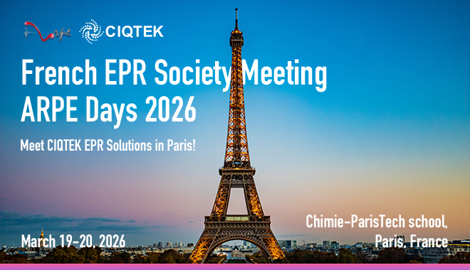
CIQTEK is pleased to announce its participation in the French EPR Society Meeting – ARPE Days 2026, taking place March 19–20, 2026, at Chimie ParisTech in Paris, France. The event brings together researchers, instrument specialists, and industry partners from across Europe to exchange the latest advances and practical applications in Electron Paramagnetic Resonance (EPR).
ARPE Days serves as an important annual gathering for the French and broader European EPR community. The meeting provides a platform for discussing developments in magnetic resonance methods, new experimental approaches, and real-world research applications across chemistry, physics, materials science, energy research, and life sciences.
For CIQTEK, the event is also an opportunity to reconnect with long-standing collaborators and meet new researchers exploring advanced EPR solutions for their laboratories.
Over the past few years, CIQTEK EPR spectrometers have been successfully delivered to multiple leading research organizations and universities across Europe, supporting work in free radical studies, catalysis, battery research, materials characterization, and quantum-related investigations.
At ARPE Days 2026, visitors will be able to learn more about CIQTEK's growing EPR portfolio, including:
Benchtop EPR systems, offering compact, cost-effective solutions for routine measurements and teaching labs
High-performance CW EPR spectrometers for advanced research applications
Pulse EPR systems supporting more sophisticated spin dynamics and structure investigations
Q-band and W-band EPR solutions for higher resolution and sensitivity in cutting-edge research fields
Supporting accessories and upgrades, including temperature control and application-driven configurations
In addition to new systems, CIQTEK also provides EPR modernization and upgrade solutions, enabling laboratories to extend the lifetime and capabilities of existing instruments through electronics, control system, and performance upgrades without requiring full instrument replacement.
Researchers interested in practical use cases can also explore , where laboratories worldwide share how EPR is being used to solve real research challenges.
From energy materials to catalytic mechanisms and paramagnetic defect analysis, these stories highlight how EPR moves beyond theory into everyday lab impact. Visitors and readers are encouraged to explore the EPR Customer Stories section on the CIQTEK website to see how different research groups are applying the technology.
CIQTEK looks forward to engaging with the EPR community in Paris, exchanging ideas, and exploring future collaborations!
For more information or to schedule a meeting during the event, feel free to contact the CIQTEK team in advance.
See you in Paris this March!