Aluminum alloys, prized for their exceptional strength-to-weight ratio, are ideal materials for automotive lightweighting. Resistance spot welding (RSW) remains the mainstream joining method for automotive body manufacturing. However, the high thermal and electrical conductivity of aluminum, combined with its surface oxide layer, requires welding currents far exceeding those used for steel. This accelerates copper electrode wear, leading to unstable weld quality, frequent electrode maintenance, and increased production costs. Extending electrode life while ensuring weld quality has become a critical technological bottleneck in the industry.
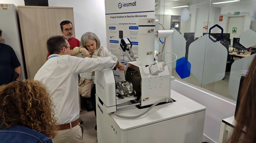
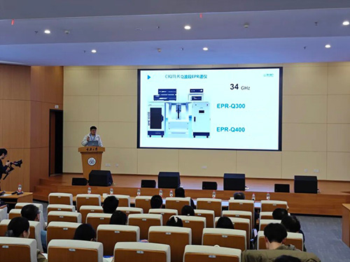
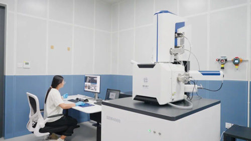
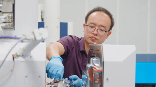
To address this challenge, Dr. Yang Shanglu's team at Shanghai Institute of Optics and Fine Mechanics conducted an in-depth study using the CIQTEK FESEM SEM5000. They innovatively designed a raised-ring electrode and systematically investigated the effect of ring number (0–4) on electrode morphology, revealing the intrinsic relationship between ring count, crystal defects in the weld nugget, and current distribution. Their results show that increasing the number of raised rings optimizes current distribution, improves thermal input efficiency, enlarges the weld nugget, and significantly extends electrode lifespan. Notably, the raised rings enhance oxide layer penetration, improving current flow while reducing pitting corrosion. This innovative electrode design provides a new technical approach for mitigating electrode wear and lays a theoretical and practical foundation for broader application of aluminum alloy RSW in the automotive industry. The study is published in the Journal of Materials Processing Tech. under the title “Investigating the Influence of Electrode Surface Morphology on Aluminum Alloy Resistance Spot Welding.”
Raised-Ring Electrode Design Breakthrough
Facing the electrode wear challenge, the team approached the problem from electrode morphology. They machined 0 to 4 concentric raised rings on the end face of conventional spherical electrodes, forming a novel Newton Ring electrode (NTR).
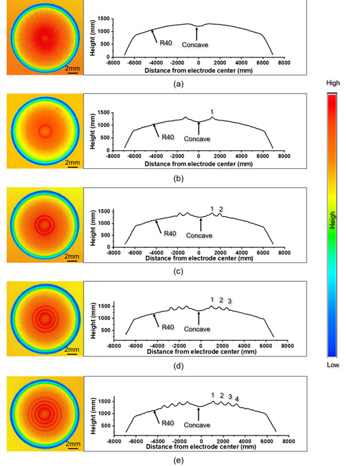 Figure 1. Surface morphology and cross-sectional profile of the electrodes used in the experiment
SEM Analysis Reveals Crystal Defects and Performance Enhancement
How do raised rings influence welding performance? Using the CIQTEK FESEM SEM5000 and EBSD techniques, the team characterized the microstructure of weld nuggets in detail. They found that the raised rings pierce the aluminum oxide layer during welding, optimizing current distribution, influencing heat input, and promoting nugget growth. More importantly, the mechanical interaction between raised rings and molten metal significantly increases the density of crystal defects, such as geometrically necessary dislocations (GNDs) and low-angle grain boundaries (LAGBs), within the weld nugget. Optimal performance was observed with three raised rings (NTR3).
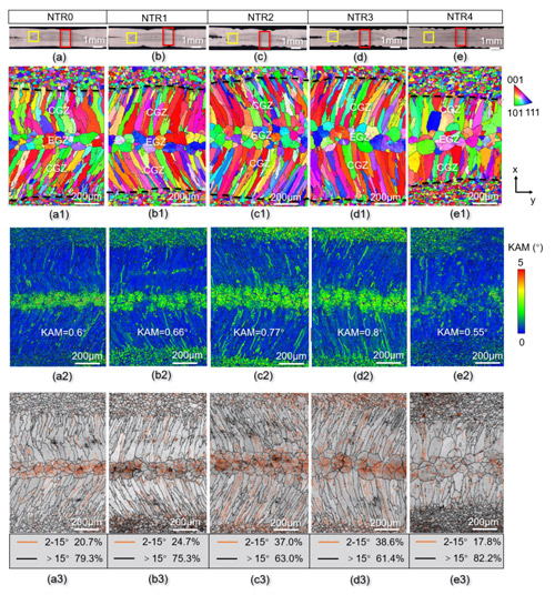
Figure 2. EBSD analysis of weld nugget microstructure for NTR0, NTR1, NTR2, NTR3, and NTR4 electrodes
Prolonged Electrode Life
Beyond improving weld quality, the raised-ring electrodes demonstrate outstanding anti-abrasion performance. After a 10-weld lifespan test, the difference in electrode wear was striking.
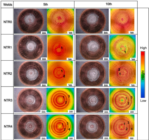 Figure 3. Electrode lifespan for NTR0, NTR1, NTR2, NTR3, and NTR4 electrodes
Quantitative Analysis
The NTR0 electrode without raised rings exhibited a wear area of 13.49 million μm².
In comparison, NTR3 and NTR4 electrodes with three and four raised rings reduced wear areas to 4.35 million μm² and 3.98 million μm², representing reductions of 67.8% and 70.5%, respectively.
The raised-ring structure concentrates current along the rings, guiding wear along predetermined paths and preventing random pit expansion, effectively doubling electrode lifespan.
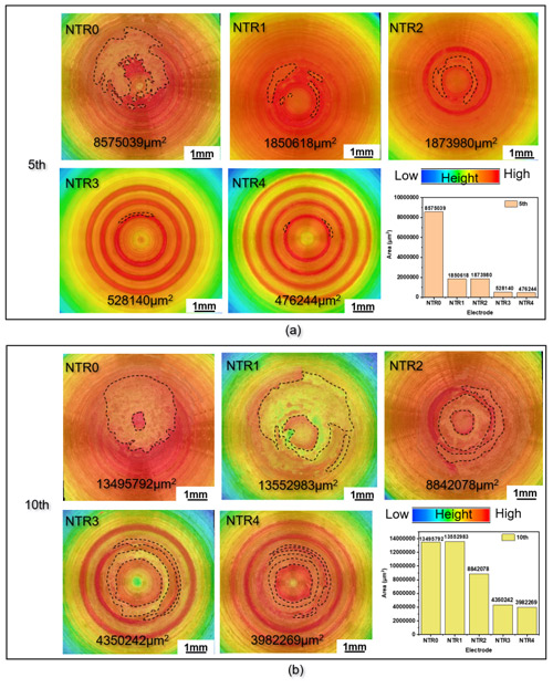 Figure 4. Pitting area of NTR0, NTR1, NTR2, NTR3, and NTR4 electrodes after 5 and 10 welds: (a) 5th weld, (b) 10th weld、
Microanalysis of Electrode Pitting
Further SEM analysis of NTR0 electrodes after welding until adhesion to the aluminum sheet revealed a 10 μm-thick intermetallic compound (IMC) layer between the electrode and the sheet. This transition layer consists of two copper-containing sublayers:
Near the electrode: thinner sublayer with 29.2 at.% Cu (Al4Cu9 phase).
Near the aluminum alloy: thicker sublayer with 15.5 at.% Cu (AlCu2 phase).
 Figure 5. Composition analysis of pitting between the electrode and the sheet
This study demonstrates that innovative electrode morphology can effectively regulate current distribution, improving weld quality while extending electrode life. CIQTEK FESEM microscope provided indispensable visualization and quantitative evidence of microscopic mechanisms, including crystal defect evolution and electrode pitting, highlighting the critical role of advanced characterization in advancing welding research and industrial applications.