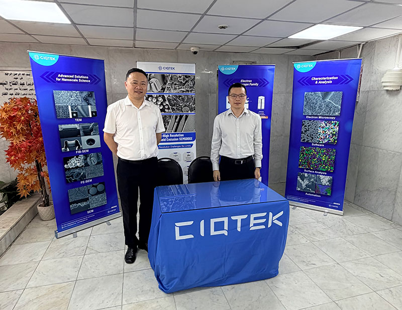
CIQTEK continues to expand its presence in Europe with the establishment of an SEM demo station in Spain, operated by the trusted local distributor IESMAT. Located in Madrid, the demo station features a CIQTEK High-Performance and Universal Tungsten Filament SEM Microscope SEM3200, providing Spanish users with convenient access to live demonstrations, sample testing, and hands-on operation. The facility also offers professional Spanish-language service and technical consultation, helping local customers better understand and apply CIQTEK’s advanced electron microscopy technologies.
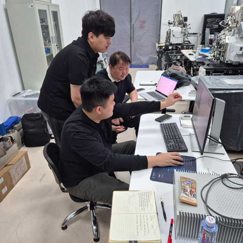
Since the installation of the CIQTEK SEM3200, IESMAT has actively organized a series of seminars and workshops throughout 2025, typically held every one to two months. These events welcome researchers and professionals from academia and industry to explore the performance and advantages of CIQTEK scanning electron microscopes through hands-on sessions and interactive learning experiences.
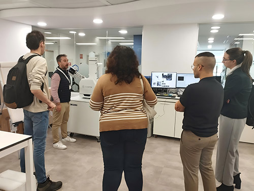 IESMAT SEM Workshop in January 2025
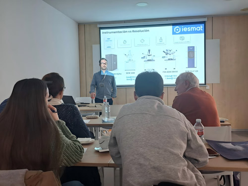 IESMAT SEM Seminar in Feb, 2025
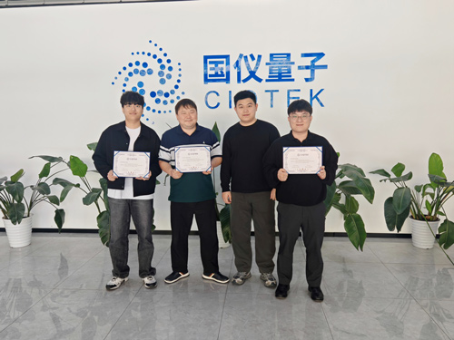
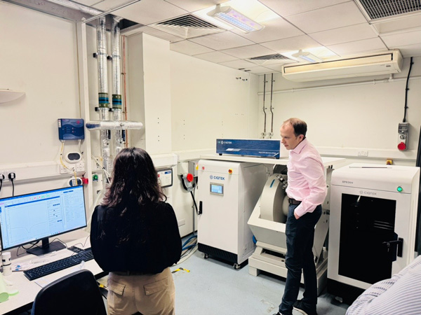
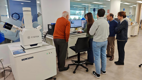 IESMAT Most Recent SEM Seminar in Sep, 2025
The next event, IESMAT Electron Microscopy Day II, will take place on November 6, 2025, in Madrid. Participants will enjoy:
-
Live hands-on electron microscopy with the CIQTEK SEM3200
-
Cutting-edge analytics using EDS and EBSD
-
Insights into current trends and future directions of electron microscopy in Spain
The SEM demo station at IESMAT marks an important milestone in CIQTEK’s European development strategy. It enhances local accessibility to advanced electron microscopy technologies and provides researchers with authentic, real-world experience. Through close collaboration with partners like IESMAT, CIQTEK is deepening its engagement with the European market, promoting innovation, and building stronger connections with the scientific community.
CIQTEK remains committed to empowering global users through advanced instrumentation, localized service, and continuous collaboration for scientific progress.