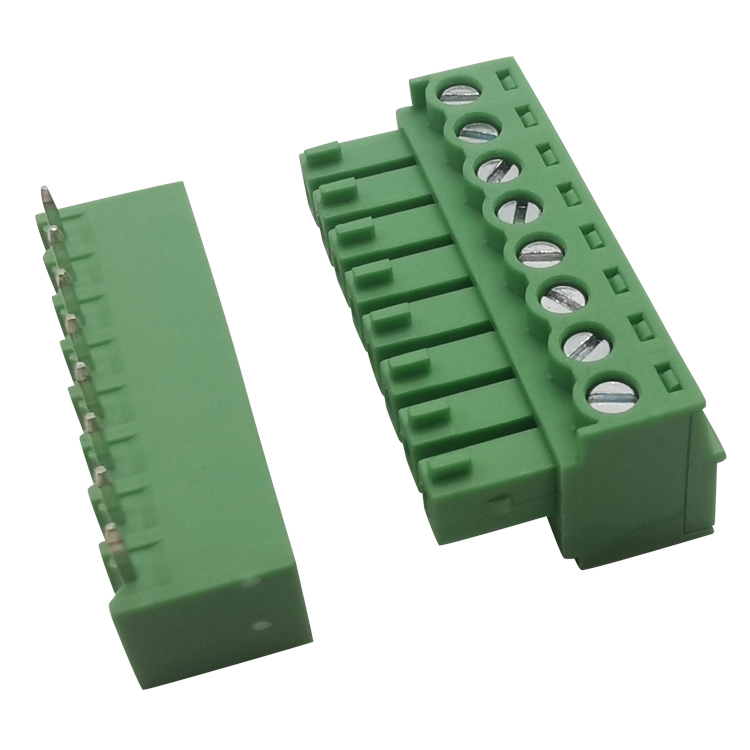
When it comes to terminal blocks, the HONG YI 5.08 Terminal Block stands out for its superior manufacturing process. With the use of advanced technology and precise craftsmanship, this terminal block ensures reliable connections in various electronic applications. In this article, we will delve into the key factors that make the HONG YI pcb screw connector the preferred choice in the industry.
Benefits of the PCB Screw Connector:
In modern electronic designs, a secure and stable connection is crucial. The HONG YI 5.08 Terminal Block incorporates a high-quality PCB screw connector, ensuring a secure and reliable connection between the terminal block and the PCB. This feature guarantees long-term stability and facilitates easy maintenance.

Understanding the 5.08 Terminal Block:
The 5.08 terminal block is a widely used connector type in the electronics industry. Featuring a 5.08 mm pitch, it provides ample space for secure wire connections. The HONG YI 5.08 connector adheres to the industry-standard dimensions and specifications, making it compatible with various applications and suitable for different project requirements.
Versatility of the 5.08 Connector:
One of the key advantages of the 5.08 mm connector is its versatility. With the ability to accommodate different wire sizes and types, this connector offers flexibility in connection options. Whether you are working with solid or stranded wires, the HONG YI 5.08 Terminal Block provides a reliable and efficient solution for your connectivity needs.
Precise Design of the 5.08 mm Connector:
The HONG YI 5.08 Terminal Block excels in precision engineering. Every aspect of the 5.08 mm connector is designed with meticulous attention to detail. From the robust housing material to the well-defined contact points, this terminal block ensures optimal electrical performance and minimizes the risk of signal loss.
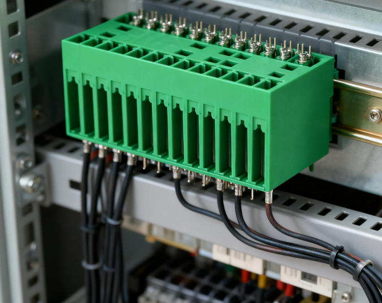
The Advantages of Terminal Block 5.08:
Terminal block 5.08 offers unrivaled reliability and durability. Designed for demanding industrial environments, it can withstand challenging operating conditions such as temperature fluctuations and mechanical stress. With its rugged construction and excellent electrical properties, the HONG YI 5.08 Terminal Block ensures consistent performance and longevity.
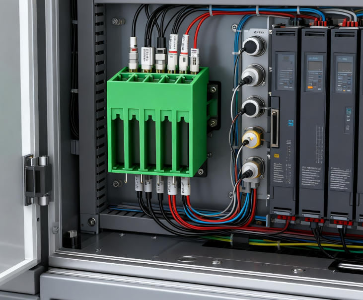
Terminal Block 5.08 mm for Efficient Connectivity:
The HONG YI 5.08 Terminal Block is engineered to streamline the connectivity process. With its user-friendly design and easy wiring options, it enables efficient installation and maintenance. Whether you are working on a small-scale project or a large-scale industrial application, this terminal block simplifies the connectivity workflow, saving time and effort.
In the realm of terminal block manufacturing, the HONG YI 5.08 Terminal Block sets the standard for excellence. With its PCB screw connector, precise design, versatility, and robust construction, this terminal block delivers reliable and efficient connectivity. When it comes to electrical connections, trust the HONG YI 5.08 Terminal Block to provide secure and long-lasting performance for your electronic projects.