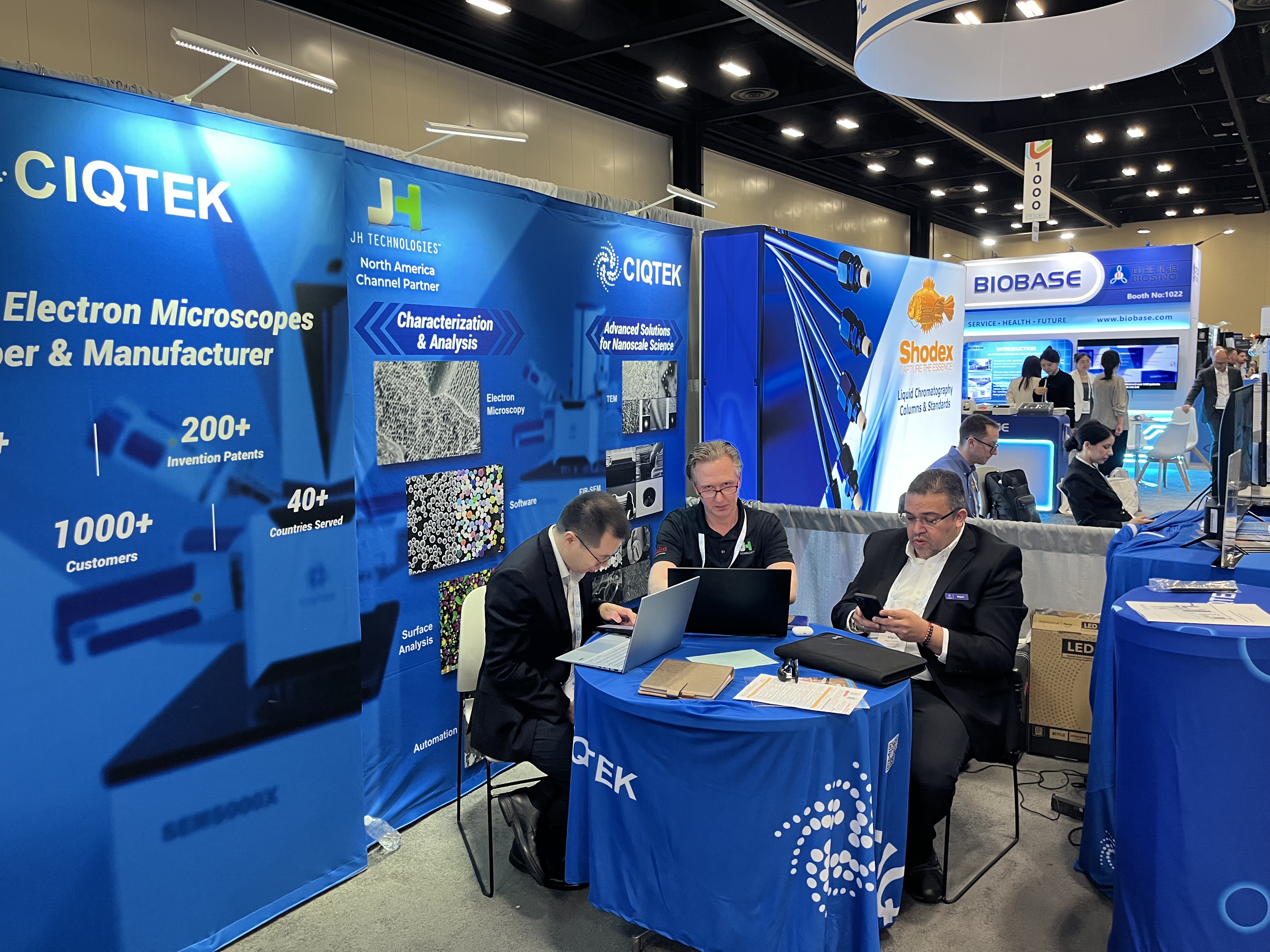
CIQTEK successfully participated in Pittcon 2026, March 9–11, San Antonio, TX, connecting with researchers, instrument specialists, and industry professionals from across North America and around the world.
At booth #1113, the CIQTEK team presented its latest solutions in electron microscopy, NMR and EPR spectroscopy, and gas adsorption analysis, drawing strong interest from visitors working in materials science, chemistry, and advanced research.
Supported by the CIQTEK U.S. team and local distribution partners, the booth provided a welcoming space for in-depth technical discussions and live demonstrations. Many visitors stopped by to learn more about CIQTEK instruments and explore how these technologies can support their research projects.
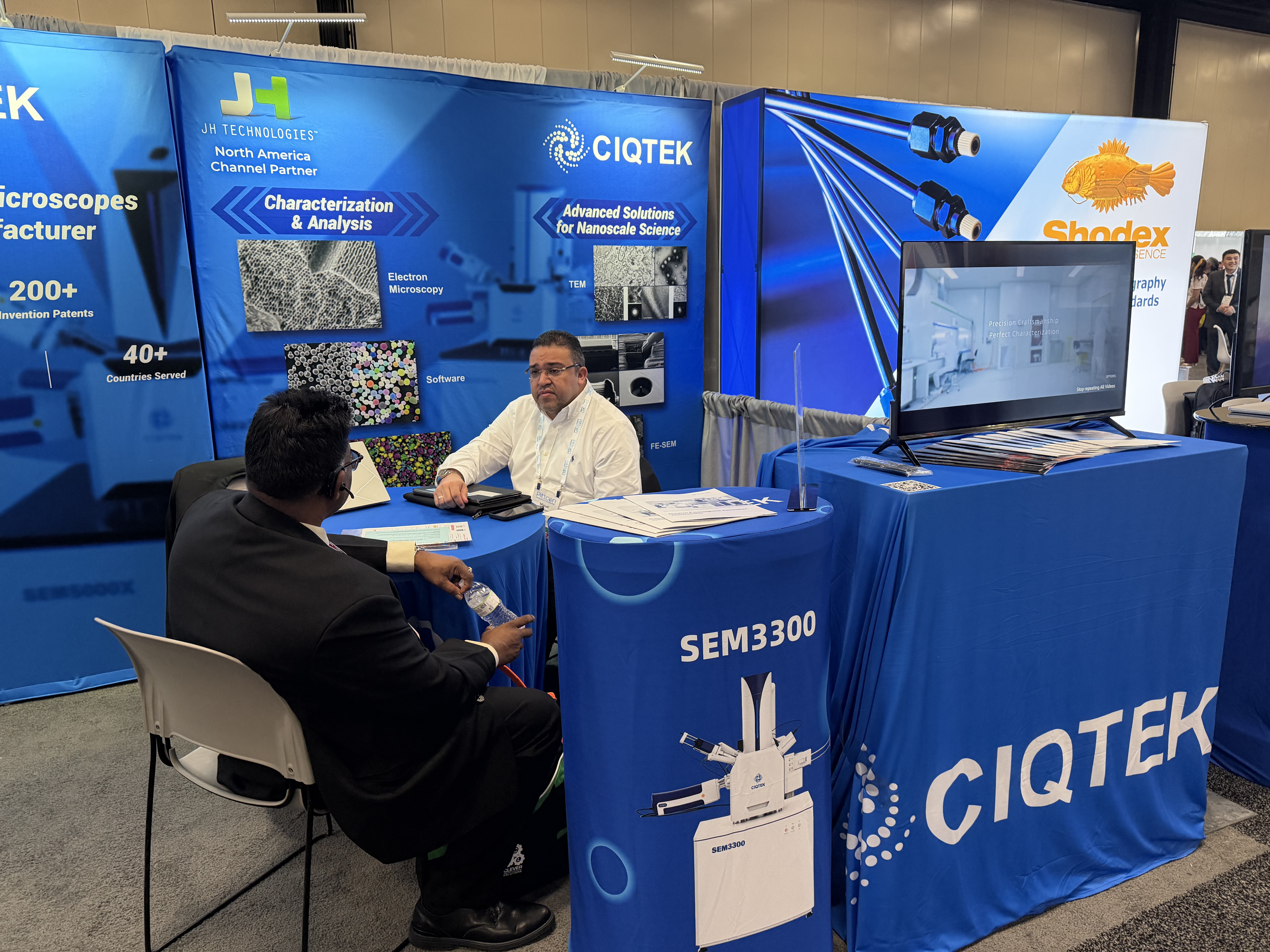
Showcasing CIQTEK Electron Microscopy
Electron microscopy was one of the key highlights at the CIQTEK booth. Visitors had the opportunity to learn about CIQTEK electron microscopy (SEM/FIB, TEM) solutions, designed to provide reliable high-resolution imaging for a wide range of applications.
Researchers from universities and research laboratories were particularly interested in how CIQTEK SEM systems can support materials characterization, nanostructure analysis, and semiconductor research. The CIQTEK team shared real application examples and discussed how stable imaging performance and user-friendly operation can help laboratories obtain high-quality results more efficiently.
NMR and EPR Spectroscopy for Modern Research
CIQTEK also introduced its portfolio of Nuclear Magnetic Resonance (NMR) and Electron Paramagnetic Resonance (EPR) spectrometers, which attracted strong interest from scientists in chemistry, catalysis, and materials research.
Many visitors were interested in CIQTEK benchtop EPR solutions, designed to make EPR spectroscopy more accessible to laboratories seeking compact systems with strong performance. Discussions at the booth covered a range of applications, including studies of free radicals, transition metal ions, and material defects.
Surface and Porosity Analysis
In addition to electron microscopy and EPR, CIQTEK presented its gas adsorption analyzers for surface area and pore structure characterization. These instruments are widely used in research areas such as catalysts, energy materials, porous materials, and environmental science.
Visitors were interested in discussing measurement workflows, data interpretation, and how gas adsorption techniques can complement other characterization methods in materials research.
Strengthening Connections in North America
With support from the CIQTEK U.S. team and local partners, CIQTEK continues to expand its presence in the North American market and provide responsive technical support to customers!
Contact our USA team: info.usa@ciqtek.com