Real-Time EPR Results at the Bench
For many U.S. labs, collecting data quickly and efficiently is critical. A desktop EPR brings real-time EPR spin analysis into everyday workflows, allowing scientists to move from sample preparation to results faster. Researchers can monitor dynamic processes such as free radical reactions, material characterization, or biological spin studies with immediate feedback.
Unlike traditional floor-standing EPR systems, a benchtop EPR allows rapid setup and operation without requiring extensive training or dedicated lab space. This makes fast EPR measurement and high-throughput spin analysis accessible for more researchers.
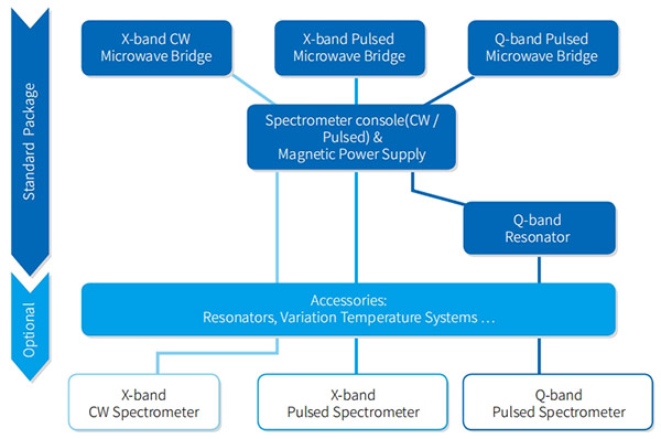
 Modern Benchtop EPR
Why Real-Time Spin Analysis Matters
Many experiments in chemistry, materials science, and biology involve species that change rapidly. Rapid EPR experiments can provide insights that would otherwise take hours or days. With a desktop EPR, researchers can:
-
Acquire spectra quickly with minimal downtime
-
Adjust experimental conditions based on real-time data
-
Iterate experiments more efficiently
-
Reduce sample waste and lab bottlenecks
By enabling real-time EPR measurement, desktop EPR systems support more agile decision-making and accelerate research cycles.
What Makes Desktop EPR Ideal for Modern Labs
Benchtop EPR spectrometers combine a compact design with high performance. Key advantages include:
- Compact EPR Form Factor
A desktop system fits on a standard lab bench, ideal for shared facilities or labs with limited space.
- Intuitive Operation
User-friendly software and controls allow researchers to perform spin analysis without specialized training, supporting multiple users in busy labs.
- Fast EPR Measurement
High-performance detection and streamlined workflows enable rapid spectral acquisition for both solid and liquid samples, making rapid EPR experiments practical.
- Reliable Performance
Modern desktop EPR systems maintain sensitivity and resolution comparable to larger instruments while providing the flexibility of a benchtop unit.
These features make desktop EPR a practical choice for labs that value efficiency and accuracy.
Real U.S. Lab Cases: Faster Workflows and Immediate Feedback in Practice
Real-time EPR is not just a theoretical advantage. In several U.S. research laboratories, desktop EPR systems are already being used to shorten experiment cycles and deliver immediate data feedback, especially in environments where access to large shared instruments is limited or inefficient.
At Cornell University, a CIQTEK benchtop EPR system was introduced to support both biomedical research and teaching. One of the key motivations was workflow efficiency. Instead of scheduling time on a centralized EPR facility, researchers could perform spin analysis directly at the lab bench, immediately after sample preparation. This allowed rapid checks of radical signals and faster decisions on whether experiments should proceed, repeat, or be adjusted. For students and researchers alike, real-time EPR access reduced waiting time and made data interpretation part of the same working session, rather than a separate step days later.
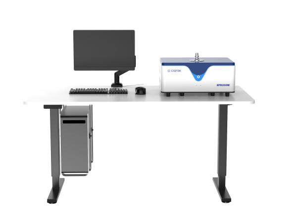
A similar efficiency-driven approach can be seen at Northwestern University, where a CIQTEK desktop EPR200M is used in materials and chemistry research. Researchers value the ability to run fast EPR measurements without interrupting ongoing experiments. Having a benchtop EPR nearby enables quick verification of paramagnetic species during synthesis or material processing, helping teams respond immediately to unexpected results and optimize conditions on the spot.
At the University of Texas at Dallas, the adoption of the CIQTEK desktop EPR system supports both research and instructional use. For teaching labs and student projects, real-time EPR measurements mean that experiments can be completed and discussed within a single lab session. For research users, the system provides rapid feedback during routine spin analysis, improving throughput and reducing dependency on shared, high-demand instrumentation.
Across these U.S. labs, the common theme is not simply access to EPR, but speed and control over the experimental timeline. Desktop EPR systems allow researchers to move from sample to spectrum quickly, integrate data analysis into daily workflows, and maintain momentum in fast-paced research environments.
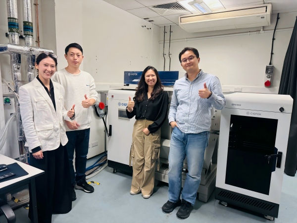
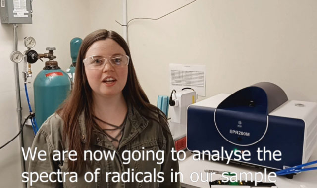 A screenshot from a user feedback video of the CIQTEK desktop EPR200M from Cornell University
How Desktop EPR Boosts Laboratory Productivity
Integrating a benchtop EPR into lab workflows can transform research efficiency. Key benefits include:
-
Shorter setup and measurement times
-
Faster turnaround for real-time EPR experiments
-
Ability to handle higher sample throughput
-
Flexibility for both research and teaching applications
With desktop EPR, labs can achieve rapid EPR experiments and continuous data flow without waiting for traditional instruments.
Performance and Value in One System
A desktop EPR spectrometer delivers strong, high-performance EPR capabilities at a significantly lower cost than many legacy systems. The combination of compact design, quick measurement, and streamlined operation makes benchtop EPR an attractive option for laboratories that need reliable spin analysis without heavy infrastructure or long setup times.
Within this category, CIQTEK desktop EPR systems stand out for their exceptional price-to-performance balance. By focusing on the core measurement needs of modern research labs, CIQTEK offers benchtop EPR instruments that provide robust sensitivity, stable performance, and real-time data access at a price point that is difficult to match. This allows more research groups to adopt EPR spectroscopy as a routine tool rather than a limited shared resource.
For U.S. laboratories conducting spin analysis, CIQTEK benchtop EPR systems deliver immediate results from bench to insight, helping teams maximize research output while keeping capital investment under control. The result is a practical, efficient solution that aligns with both scientific goals and budget realities.